- 您現(xiàn)在的位置:買賣IC網(wǎng) > PDF目錄369923 > MPC106 (Motorola, Inc.) 32-Bit Microprocessor(32位微處理器) PDF資料下載
參數(shù)資料
| 型號: | MPC106 |
| 廠商: | Motorola, Inc. |
| 英文描述: | 32-Bit Microprocessor(32位微處理器) |
| 中文描述: | 32位微處理器(32位微處理器) |
| 文件頁數(shù): | 222/398頁 |
| 文件大小: | 1112K |
| 代理商: | MPC106 |
第1頁第2頁第3頁第4頁第5頁第6頁第7頁第8頁第9頁第10頁第11頁第12頁第13頁第14頁第15頁第16頁第17頁第18頁第19頁第20頁第21頁第22頁第23頁第24頁第25頁第26頁第27頁第28頁第29頁第30頁第31頁第32頁第33頁第34頁第35頁第36頁第37頁第38頁第39頁第40頁第41頁第42頁第43頁第44頁第45頁第46頁第47頁第48頁第49頁第50頁第51頁第52頁第53頁第54頁第55頁第56頁第57頁第58頁第59頁第60頁第61頁第62頁第63頁第64頁第65頁第66頁第67頁第68頁第69頁第70頁第71頁第72頁第73頁第74頁第75頁第76頁第77頁第78頁第79頁第80頁第81頁第82頁第83頁第84頁第85頁第86頁第87頁第88頁第89頁第90頁第91頁第92頁第93頁第94頁第95頁第96頁第97頁第98頁第99頁第100頁第101頁第102頁第103頁第104頁第105頁第106頁第107頁第108頁第109頁第110頁第111頁第112頁第113頁第114頁第115頁第116頁第117頁第118頁第119頁第120頁第121頁第122頁第123頁第124頁第125頁第126頁第127頁第128頁第129頁第130頁第131頁第132頁第133頁第134頁第135頁第136頁第137頁第138頁第139頁第140頁第141頁第142頁第143頁第144頁第145頁第146頁第147頁第148頁第149頁第150頁第151頁第152頁第153頁第154頁第155頁第156頁第157頁第158頁第159頁第160頁第161頁第162頁第163頁第164頁第165頁第166頁第167頁第168頁第169頁第170頁第171頁第172頁第173頁第174頁第175頁第176頁第177頁第178頁第179頁第180頁第181頁第182頁第183頁第184頁第185頁第186頁第187頁第188頁第189頁第190頁第191頁第192頁第193頁第194頁第195頁第196頁第197頁第198頁第199頁第200頁第201頁第202頁第203頁第204頁第205頁第206頁第207頁第208頁第209頁第210頁第211頁第212頁第213頁第214頁第215頁第216頁第217頁第218頁第219頁第220頁第221頁當(dāng)前第222頁第223頁第224頁第225頁第226頁第227頁第228頁第229頁第230頁第231頁第232頁第233頁第234頁第235頁第236頁第237頁第238頁第239頁第240頁第241頁第242頁第243頁第244頁第245頁第246頁第247頁第248頁第249頁第250頁第251頁第252頁第253頁第254頁第255頁第256頁第257頁第258頁第259頁第260頁第261頁第262頁第263頁第264頁第265頁第266頁第267頁第268頁第269頁第270頁第271頁第272頁第273頁第274頁第275頁第276頁第277頁第278頁第279頁第280頁第281頁第282頁第283頁第284頁第285頁第286頁第287頁第288頁第289頁第290頁第291頁第292頁第293頁第294頁第295頁第296頁第297頁第298頁第299頁第300頁第301頁第302頁第303頁第304頁第305頁第306頁第307頁第308頁第309頁第310頁第311頁第312頁第313頁第314頁第315頁第316頁第317頁第318頁第319頁第320頁第321頁第322頁第323頁第324頁第325頁第326頁第327頁第328頁第329頁第330頁第331頁第332頁第333頁第334頁第335頁第336頁第337頁第338頁第339頁第340頁第341頁第342頁第343頁第344頁第345頁第346頁第347頁第348頁第349頁第350頁第351頁第352頁第353頁第354頁第355頁第356頁第357頁第358頁第359頁第360頁第361頁第362頁第363頁第364頁第365頁第366頁第367頁第368頁第369頁第370頁第371頁第372頁第373頁第374頁第375頁第376頁第377頁第378頁第379頁第380頁第381頁第382頁第383頁第384頁第385頁第386頁第387頁第388頁第389頁第390頁第391頁第392頁第393頁第394頁第395頁第396頁第397頁第398頁
6-2
MPC106 PCIB/MC User's Manual
MOTOROLA
The ROM/Flash interface supports one or two banks of ROM/Flash memory on the
60x/memory bus. Bank sizes up to 8 Mbytes provide for a maximum ROM/Flash memory
size of 16 Mbytes. The ROM space may also be mapped to the PCI bus or split between the
60x/memory bus and the PCI bus.
6.2 Memory Interface Signal Buffering
To reduce loading on the data bus, most system designs will require buffering between the
60x data bus and the memory data bus. The MPC106 features configurable data buffer
control logic to accommodate flow-through, transparent latch, or registered data buffers.
This section describes the different buffer control configurations of the MPC106. Note that
in addition to the data and parity signals, certain other memory interface signals may also
require buffering. The AC characteristics of the MPC106, memory operating frequency,
capacitive loading, and transmission line effects of the board layout dictate which signals
require buffering, and which buffer devices are appropriate. The example design in
Figure 6-4 uses bidirectional/tri-state drivers on the data and parity signals.
The BCTL0 and BCTL1 signals control the data bus buffers (directional control and
high-impedance state). The buffer mode parameter (MCCR2[BUF_MODE]) controls how
the buffer control signals, BCTL0 and BCTL1, operate. The memory buffer type
parameters (MCCR4[WCBUF] and MCCR4[RCBUF]) determines the type of buffer used
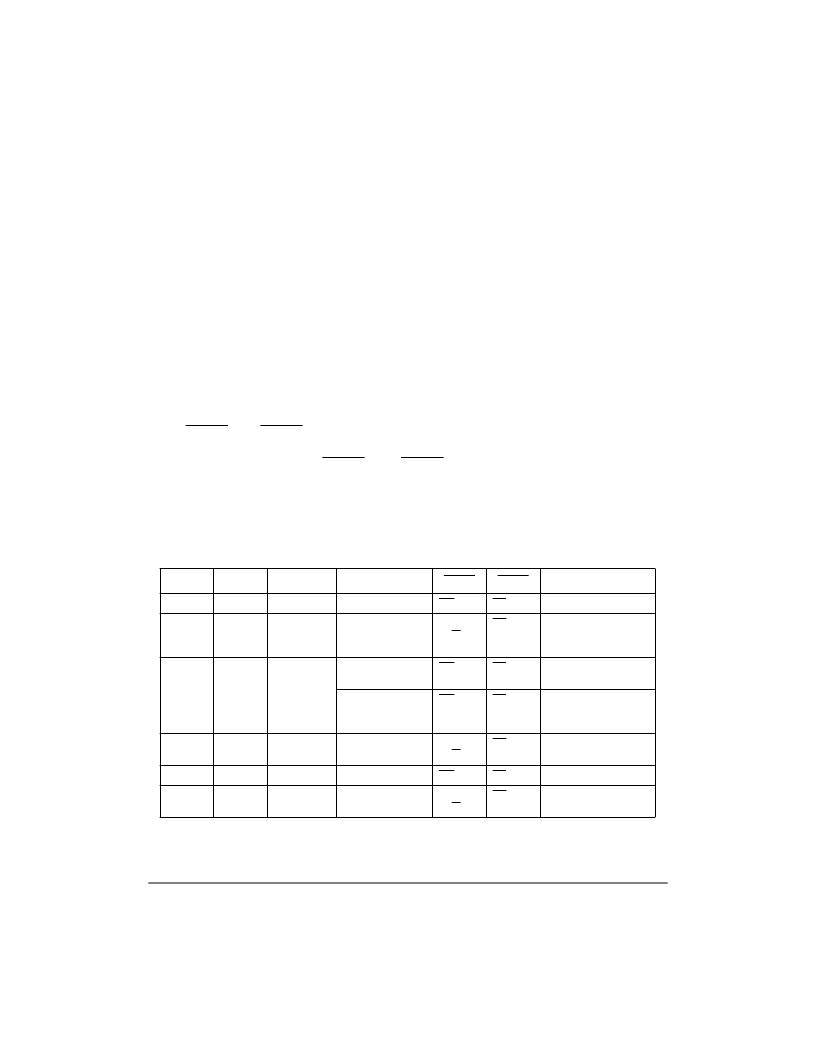
and the data synchronization for that buffer type. Table 6-1 shows the parameter settings for
the different configurations and gives examples of typical buffer devices that might be used
in those configurations.
Table 6-1. Buffer Configurations
WCBUF
RCBUF
BUF_MODE
Buffer Type
BCTL0
BCTL1
Typical Buffer Device
0
0
0
Flow-through
WE
RE
54/7416863
0
0
1
Flow-through
DIR
(R/W)
OE
54/7416245
54/74162245
54/74163245
0
1
0
Transparent latch
(DRAM/EDO)
WE
RE
54/7416543
54/74162543
Registered
(DRAM/EDO)
WE
RE
54/7416952
54/74162952
54/7416601
0
1
1
—
DIR
(R/W)
OE
—
1
0
0
—
WE
RE
—
1
0
1
—
DIR
(R/W)
OE
—
相關(guān)PDF資料 |
PDF描述 |
|---|---|
| MPC107 | 32-Bit Microprocessor(32位微處理器) |
| MPC505 | Highly Integrated, Low-Power, 32-Bit Microcontroller |
| MPC509 | Highly Integrated, Low-Power, 32-Bit Microcontroller |
| MPC5200BV400 | MPC5200 Hardware Specifications |
| MPC5200CBV266 | MPC5200 Hardware Specifications |
相關(guān)代理商/技術(shù)參數(shù) |
參數(shù)描述 |
|---|---|
| MPC106ARX66CE | 制造商:MOTOROLA 制造商全稱:Motorola, Inc 功能描述:PCI Bridge/Memory Controller |
| MPC106ARX66CG | 制造商:Freescale Semiconductor 功能描述: 制造商:Motorola Inc 功能描述: |
| MPC106ARX66DE | 制造商:MOTOROLA 制造商全稱:Motorola, Inc 功能描述:PCI Bridge/Memory Controller |
| MPC106ARX66DG | 制造商:MOTOROLA 制造商全稱:Motorola, Inc 功能描述:PCI Bridge/Memory Controller |
| MPC106ARX66TE | 制造商:MOTOROLA 制造商全稱:Motorola, Inc 功能描述:PCI Bridge/Memory Controller |
發(fā)布緊急采購,3分鐘左右您將得到回復(fù)。