- 您現(xiàn)在的位置:買(mǎi)賣(mài)IC網(wǎng) > PDF目錄377000 > DSP16410C TVS 400W 7.0V UNIDIRECT SMA PDF資料下載
參數(shù)資料
| 型號(hào): | DSP16410C |
| 英文描述: | TVS 400W 7.0V UNIDIRECT SMA |
| 中文描述: | DSP1629數(shù)字信號(hào)處理器 |
| 文件頁(yè)數(shù): | 8/373頁(yè) |
| 文件大?。?/td> | 5643K |
| 代理商: | DSP16410C |
第1頁(yè)第2頁(yè)第3頁(yè)第4頁(yè)第5頁(yè)第6頁(yè)第7頁(yè)當(dāng)前第8頁(yè)第9頁(yè)第10頁(yè)第11頁(yè)第12頁(yè)第13頁(yè)第14頁(yè)第15頁(yè)第16頁(yè)第17頁(yè)第18頁(yè)第19頁(yè)第20頁(yè)第21頁(yè)第22頁(yè)第23頁(yè)第24頁(yè)第25頁(yè)第26頁(yè)第27頁(yè)第28頁(yè)第29頁(yè)第30頁(yè)第31頁(yè)第32頁(yè)第33頁(yè)第34頁(yè)第35頁(yè)第36頁(yè)第37頁(yè)第38頁(yè)第39頁(yè)第40頁(yè)第41頁(yè)第42頁(yè)第43頁(yè)第44頁(yè)第45頁(yè)第46頁(yè)第47頁(yè)第48頁(yè)第49頁(yè)第50頁(yè)第51頁(yè)第52頁(yè)第53頁(yè)第54頁(yè)第55頁(yè)第56頁(yè)第57頁(yè)第58頁(yè)第59頁(yè)第60頁(yè)第61頁(yè)第62頁(yè)第63頁(yè)第64頁(yè)第65頁(yè)第66頁(yè)第67頁(yè)第68頁(yè)第69頁(yè)第70頁(yè)第71頁(yè)第72頁(yè)第73頁(yè)第74頁(yè)第75頁(yè)第76頁(yè)第77頁(yè)第78頁(yè)第79頁(yè)第80頁(yè)第81頁(yè)第82頁(yè)第83頁(yè)第84頁(yè)第85頁(yè)第86頁(yè)第87頁(yè)第88頁(yè)第89頁(yè)第90頁(yè)第91頁(yè)第92頁(yè)第93頁(yè)第94頁(yè)第95頁(yè)第96頁(yè)第97頁(yè)第98頁(yè)第99頁(yè)第100頁(yè)第101頁(yè)第102頁(yè)第103頁(yè)第104頁(yè)第105頁(yè)第106頁(yè)第107頁(yè)第108頁(yè)第109頁(yè)第110頁(yè)第111頁(yè)第112頁(yè)第113頁(yè)第114頁(yè)第115頁(yè)第116頁(yè)第117頁(yè)第118頁(yè)第119頁(yè)第120頁(yè)第121頁(yè)第122頁(yè)第123頁(yè)第124頁(yè)第125頁(yè)第126頁(yè)第127頁(yè)第128頁(yè)第129頁(yè)第130頁(yè)第131頁(yè)第132頁(yè)第133頁(yè)第134頁(yè)第135頁(yè)第136頁(yè)第137頁(yè)第138頁(yè)第139頁(yè)第140頁(yè)第141頁(yè)第142頁(yè)第143頁(yè)第144頁(yè)第145頁(yè)第146頁(yè)第147頁(yè)第148頁(yè)第149頁(yè)第150頁(yè)第151頁(yè)第152頁(yè)第153頁(yè)第154頁(yè)第155頁(yè)第156頁(yè)第157頁(yè)第158頁(yè)第159頁(yè)第160頁(yè)第161頁(yè)第162頁(yè)第163頁(yè)第164頁(yè)第165頁(yè)第166頁(yè)第167頁(yè)第168頁(yè)第169頁(yè)第170頁(yè)第171頁(yè)第172頁(yè)第173頁(yè)第174頁(yè)第175頁(yè)第176頁(yè)第177頁(yè)第178頁(yè)第179頁(yè)第180頁(yè)第181頁(yè)第182頁(yè)第183頁(yè)第184頁(yè)第185頁(yè)第186頁(yè)第187頁(yè)第188頁(yè)第189頁(yè)第190頁(yè)第191頁(yè)第192頁(yè)第193頁(yè)第194頁(yè)第195頁(yè)第196頁(yè)第197頁(yè)第198頁(yè)第199頁(yè)第200頁(yè)第201頁(yè)第202頁(yè)第203頁(yè)第204頁(yè)第205頁(yè)第206頁(yè)第207頁(yè)第208頁(yè)第209頁(yè)第210頁(yè)第211頁(yè)第212頁(yè)第213頁(yè)第214頁(yè)第215頁(yè)第216頁(yè)第217頁(yè)第218頁(yè)第219頁(yè)第220頁(yè)第221頁(yè)第222頁(yè)第223頁(yè)第224頁(yè)第225頁(yè)第226頁(yè)第227頁(yè)第228頁(yè)第229頁(yè)第230頁(yè)第231頁(yè)第232頁(yè)第233頁(yè)第234頁(yè)第235頁(yè)第236頁(yè)第237頁(yè)第238頁(yè)第239頁(yè)第240頁(yè)第241頁(yè)第242頁(yè)第243頁(yè)第244頁(yè)第245頁(yè)第246頁(yè)第247頁(yè)第248頁(yè)第249頁(yè)第250頁(yè)第251頁(yè)第252頁(yè)第253頁(yè)第254頁(yè)第255頁(yè)第256頁(yè)第257頁(yè)第258頁(yè)第259頁(yè)第260頁(yè)第261頁(yè)第262頁(yè)第263頁(yè)第264頁(yè)第265頁(yè)第266頁(yè)第267頁(yè)第268頁(yè)第269頁(yè)第270頁(yè)第271頁(yè)第272頁(yè)第273頁(yè)第274頁(yè)第275頁(yè)第276頁(yè)第277頁(yè)第278頁(yè)第279頁(yè)第280頁(yè)第281頁(yè)第282頁(yè)第283頁(yè)第284頁(yè)第285頁(yè)第286頁(yè)第287頁(yè)第288頁(yè)第289頁(yè)第290頁(yè)第291頁(yè)第292頁(yè)第293頁(yè)第294頁(yè)第295頁(yè)第296頁(yè)第297頁(yè)第298頁(yè)第299頁(yè)第300頁(yè)第301頁(yè)第302頁(yè)第303頁(yè)第304頁(yè)第305頁(yè)第306頁(yè)第307頁(yè)第308頁(yè)第309頁(yè)第310頁(yè)第311頁(yè)第312頁(yè)第313頁(yè)第314頁(yè)第315頁(yè)第316頁(yè)第317頁(yè)第318頁(yè)第319頁(yè)第320頁(yè)第321頁(yè)第322頁(yè)第323頁(yè)第324頁(yè)第325頁(yè)第326頁(yè)第327頁(yè)第328頁(yè)第329頁(yè)第330頁(yè)第331頁(yè)第332頁(yè)第333頁(yè)第334頁(yè)第335頁(yè)第336頁(yè)第337頁(yè)第338頁(yè)第339頁(yè)第340頁(yè)第341頁(yè)第342頁(yè)第343頁(yè)第344頁(yè)第345頁(yè)第346頁(yè)第347頁(yè)第348頁(yè)第349頁(yè)第350頁(yè)第351頁(yè)第352頁(yè)第353頁(yè)第354頁(yè)第355頁(yè)第356頁(yè)第357頁(yè)第358頁(yè)第359頁(yè)第360頁(yè)第361頁(yè)第362頁(yè)第363頁(yè)第364頁(yè)第365頁(yè)第366頁(yè)第367頁(yè)第368頁(yè)第369頁(yè)第370頁(yè)第371頁(yè)第372頁(yè)第373頁(yè)
Data Addendum
May 2001
DSP16410C Digital Signal Processor
Agere Systems Inc.
8
5 Ball Grid Array Information
(continued)
5.1 208-Ball PBGA Package
(continued)
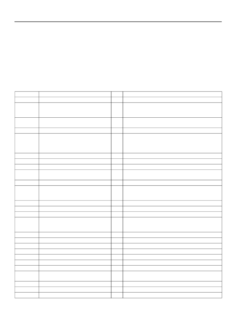
Table 2 describes the PBGA ball assignments sorted by symbol for the 208-ball package. For each signal or
power/ground connection, this table lists the PBGA coordinate, the symbol name, the type (I = input, O = output,
I/O = input/output, O/Z = 3-state output, P = power, G = ground), and description. Inputs and bidirectional pins do
not maintain full CMOS levels when not driven. They must be pulled to V
DD
2
or V
SS
through the appropriate pull
up/down resistor (refer to Section 7.1). An unused external SEMI data bus (ED[31:0]) can be statically configured
as outputs by asserting the EYMODE pin. At full CMOS levels, no significant dc current is drawn.
Table 2. 208-Ball PBGA Ball Assignments Sorted Alphabetically by Symbol
Symbol
CKI
EA[18:0]
208-Ball PBGA Coordinate
H2
H15, G13, G14, G16, G15, F16, F15,
E13, E14, E16, D14, D15, D16, C16,
C15, B16, C14, A15, B14
D12
Type
I
O
Description
External Clock Input.
External Address Bus, Bits 18
—
0.
EACKN
O
External Device Acknowledge for External Memory Inter-
face (negative assertion).
Programmable Clock Output.
External Memory Data Bus, Bits 31
—
0.
ECKO
ED[31:0]
J16
O
I/O
B11, A11, C11, D11, B10, A10, B9, C9,
D9, D8, C8, B8, D7, C7, A7, B7, A6, B6,
D5, C5, A5, C4, A4, B4, A3, B3, A2, C3,
B1, C1, C2, D2
A14
B13
E2
E1
EION
ERAMN
ERDY
EREQN
O
O
I
I
Enable for External I/O (negative assertion).
External RAM Enable (negative assertion).
External Memory Device Ready.
External Device Request for EMI Interface (negative
assertion).
Enable for External ROM (negative assertion).
EROM Type Control:
If 0, asynchronous SRAM mode.
If 1, synchronous SRAM mode.
Read/Write, Bit 0 (negative assertion).
Read/Write, Bit 1 (negative assertion).
External Segment Address, Bits 3
—
0.
External Memory Bus Size Control:
If 0, 16-bit external interface.
If 1, 32-bit external interface.
External Boot-up Control for CORE0.
External Data Bus Mode Configuration Pin.
External Interrupt Requests 3
—
0.
BIO0 Status/Control, Bits 6
—
0.
BIO1 Status/Control, Bits 6
—
0.
PIU Address, Bits 3
—
0.
PIU Chip Select (negative assertion).
PIU Data Bus, Bits 15
—
0.
EROMN
ERTYPE
B12
F2
O
I
ERWN0
ERWN1
ESEG[3:0]
ESIZE
C12
A12
O
O
O
I
J14, J13, H13, H14
E3
EXM
E4
R3
I
I
I
EYMODE
INT[3:0]
IO0BIT[6:0]
IO1BIT[6:0]
PADD[3:0]
PCSN
PD[15:0]
J3, J2, K4, K3
N3, N1, N2, P1, P2, R1, P3
T13, T14, R14, T15, P14, R16, P15
P12, T12, P13, R13
N12
T3, R4, R5, T5, P5, N5, R6, T6, P6, N6,
R7, T7, T8, P8, N8, N9
R9
T11
P10
I/O
I/O
I
I
I/O
PIBF
PIDS
PINT
O
I
O
PIU Input Buffer Full Flag.
PIU Input Data Strobe.
PIU Interrupt Request to Host.
相關(guān)PDF資料 |
PDF描述 |
|---|---|
| DSP16410 | 16-bit fixed point DSP with Flash |
| DSP25-16AR | Phase-leg Rectifier Diode |
| DSP25 | Phase-leg Rectifier Diode |
| DSP25-12A | Phase-leg Rectifier Diode |
| DSP25-12AT | Phase-leg Rectifier Diode |
相關(guān)代理商/技術(shù)參數(shù) |
參數(shù)描述 |
|---|---|
| DSP16410CG | 制造商:AGERE 制造商全稱(chēng):AGERE 功能描述:DSP16410CG Digital Signal Processor |
| DSP16411 | 制造商:AGERE 制造商全稱(chēng):AGERE 功能描述:DSP16411 Digital Signal Processor |
| DSP1643 | 制造商:未知廠家 制造商全稱(chēng):未知廠家 功能描述:Telecommunication IC |
| DSP1648C | 制造商:AGERE 制造商全稱(chēng):AGERE 功能描述:Host-Based Controller V.92 Modem Chip Set |
| DSP1675TV2RDD12VDB | 制造商:Agere Systems 功能描述: |
發(fā)布緊急采購(gòu),3分鐘左右您將得到回復(fù)。