- 您現(xiàn)在的位置:買賣IC網(wǎng) > PDF目錄377000 > DSP16410C TVS 400W 7.0V UNIDIRECT SMA PDF資料下載
參數(shù)資料
| 型號(hào): | DSP16410C |
| 英文描述: | TVS 400W 7.0V UNIDIRECT SMA |
| 中文描述: | DSP1629數(shù)字信號(hào)處理器 |
| 文件頁數(shù): | 73/373頁 |
| 文件大小: | 5643K |
| 代理商: | DSP16410C |
第1頁第2頁第3頁第4頁第5頁第6頁第7頁第8頁第9頁第10頁第11頁第12頁第13頁第14頁第15頁第16頁第17頁第18頁第19頁第20頁第21頁第22頁第23頁第24頁第25頁第26頁第27頁第28頁第29頁第30頁第31頁第32頁第33頁第34頁第35頁第36頁第37頁第38頁第39頁第40頁第41頁第42頁第43頁第44頁第45頁第46頁第47頁第48頁第49頁第50頁第51頁第52頁第53頁第54頁第55頁第56頁第57頁第58頁第59頁第60頁第61頁第62頁第63頁第64頁第65頁第66頁第67頁第68頁第69頁第70頁第71頁第72頁當(dāng)前第73頁第74頁第75頁第76頁第77頁第78頁第79頁第80頁第81頁第82頁第83頁第84頁第85頁第86頁第87頁第88頁第89頁第90頁第91頁第92頁第93頁第94頁第95頁第96頁第97頁第98頁第99頁第100頁第101頁第102頁第103頁第104頁第105頁第106頁第107頁第108頁第109頁第110頁第111頁第112頁第113頁第114頁第115頁第116頁第117頁第118頁第119頁第120頁第121頁第122頁第123頁第124頁第125頁第126頁第127頁第128頁第129頁第130頁第131頁第132頁第133頁第134頁第135頁第136頁第137頁第138頁第139頁第140頁第141頁第142頁第143頁第144頁第145頁第146頁第147頁第148頁第149頁第150頁第151頁第152頁第153頁第154頁第155頁第156頁第157頁第158頁第159頁第160頁第161頁第162頁第163頁第164頁第165頁第166頁第167頁第168頁第169頁第170頁第171頁第172頁第173頁第174頁第175頁第176頁第177頁第178頁第179頁第180頁第181頁第182頁第183頁第184頁第185頁第186頁第187頁第188頁第189頁第190頁第191頁第192頁第193頁第194頁第195頁第196頁第197頁第198頁第199頁第200頁第201頁第202頁第203頁第204頁第205頁第206頁第207頁第208頁第209頁第210頁第211頁第212頁第213頁第214頁第215頁第216頁第217頁第218頁第219頁第220頁第221頁第222頁第223頁第224頁第225頁第226頁第227頁第228頁第229頁第230頁第231頁第232頁第233頁第234頁第235頁第236頁第237頁第238頁第239頁第240頁第241頁第242頁第243頁第244頁第245頁第246頁第247頁第248頁第249頁第250頁第251頁第252頁第253頁第254頁第255頁第256頁第257頁第258頁第259頁第260頁第261頁第262頁第263頁第264頁第265頁第266頁第267頁第268頁第269頁第270頁第271頁第272頁第273頁第274頁第275頁第276頁第277頁第278頁第279頁第280頁第281頁第282頁第283頁第284頁第285頁第286頁第287頁第288頁第289頁第290頁第291頁第292頁第293頁第294頁第295頁第296頁第297頁第298頁第299頁第300頁第301頁第302頁第303頁第304頁第305頁第306頁第307頁第308頁第309頁第310頁第311頁第312頁第313頁第314頁第315頁第316頁第317頁第318頁第319頁第320頁第321頁第322頁第323頁第324頁第325頁第326頁第327頁第328頁第329頁第330頁第331頁第332頁第333頁第334頁第335頁第336頁第337頁第338頁第339頁第340頁第341頁第342頁第343頁第344頁第345頁第346頁第347頁第348頁第349頁第350頁第351頁第352頁第353頁第354頁第355頁第356頁第357頁第358頁第359頁第360頁第361頁第362頁第363頁第364頁第365頁第366頁第367頁第368頁第369頁第370頁第371頁第372頁第373頁
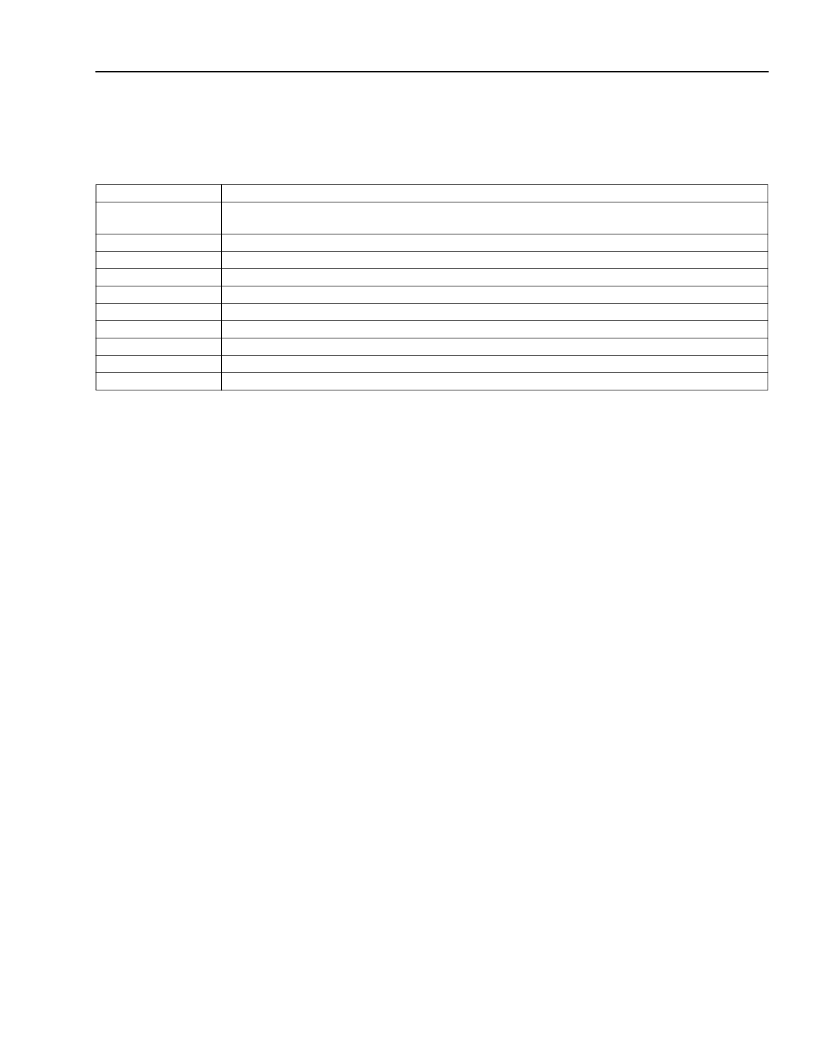
Table 1. DSP16410B Block Diagram Legend
(continued)
Data Sheet
June 2001
DSP16410B Digital Signal Processor
Agere Systems Inc.
Agere Systems—Proprietary
Use pursuant to Company instructions
17
4 Hardware Architecture
(continued)
4.1 DSP16410B Architectural Overview
(continued)
4.1.1 DSP16000 Cores
The two DSP16000 cores (CORE0 and CORE1) are
the signal processing engines of the DSP16410B. The
DSP16000 is a modified Harvard architecture with sep-
arate sets of buses for the instruction/coefficient
(X-memory) and data (Y-memory) spaces. Each set of
buses has 20 bits of address and 32 bits of data. The
core contains data and address arithmetic units and
control for on-chip memory and peripherals.
4.1.2 Clock Synthesizer (PLL)
The DSP16410B powers up with an input clock (CKI)
as the source for the processor clock (CLK). An on-
chip clock synthesizer (PLL) that runs at a frequency
multiple of CKI can also be used to generate CLK. The
clock synthesizer is deselected and powered down on
reset. The selection of the clock source is under soft-
ware control of CORE0. See
Section 4.17 beginning
on page 197
for details.
4.1.3 Triport RAMs (TPRAM
0—1
)
Each core has a private block of TPRAM consisting of
96 banks (banks 0—95) of zero wait-state memory.
Each bank consists of 1K 16-bit words and has three
separate address and data ports: one port to the core’s
instruction/coefficient (X-memory) space, a second
port to the core’s data (Y-memory) space, and a third
port to the DMA (Z-memory) space. TPRAM0 is
accessible by CORE0, TPRAM1 is accessible by
CORE1, and both TPRAM0 and TPRAM1 are accessi-
ble by the DMAU. TPRAM is organized into even and
odd interleaved banks for which each even/odd
address pair is a 32-bit wide module (see
Section 4.6
on page 43
for details). The TPRAMs support single-
word, aligned double-word, and misaligned double-
word accesses.
4.1.4 Shared Local Memory (SLM)
The SLM consists of two banks of memory. Each bank
consists of 1K 16-bit words. The SLM can be
accessed by both cores and by the DMAU and PIU
over the system bus (SAB, SDB). The SLM supports
single-word (16-bit) and aligned double-word (32-bit)
accesses. Misaligned double-word accesses are not
supported. An access to the SLM takes multiple clock
cycles to complete, and a core access to the SLM
causes the core to incur wait-states. See
Section 4.14.7.1 on page 125
for details on system bus
performance.
4.1.5 Internal Boot ROMs (IROM
0—1
)
Each core has its own boot ROM that contains a single
boot routine and software to support the Agere hard-
ware development system (HDS). The code in IROM0
and IROM1 are identical. See
Section 5 on page 205
for details.
4.1.6 Messaging Units (MGU
0—1
)
The DSP16410B provides an MGU for each core:
MGU0 for CORE0 and MGU1 for CORE1. The MGUs
provide interprocessor (core-to-core) communication
and interrupt generation. See
Section 4.8 on page 45
for details.
TPRAM
0—1
96 Kword Three-Port Random-Access Memories (one for each core). Private code (X), data (Y), and
DMA (Z).
20-Bit X-Memory Space Address Bus. One for each core.
32-Bit X-Memory Space Data Bus. One for each core.
20-Bit Y-Memory Space Address Bus. One for each core.
32-Bit Y-Memory Space Data Bus. One for each core.
20-Bit External Z-Memory Space Address Bus. Interfaces DMAU to SEMI.
32-Bit External Z-Memory Space Data Bus. Interfaces DMAU to SEMI.
20-Bit Internal Z-Memory Space Address Bus. Interfaces DMAU to TPRAM0 and TPRAM1.
32-Bit Internal Z-Memory Space Data Bus. Interfaces DMAU to TPRAM0 and TPRAM1.
External Segment Address Bits Associated with ZEAB. Interfaces DMAU to SEMI.
XAB
0—1
XDB
0—1
YAB
0—1
YDB
0—1
ZEAB
ZEDB
ZIAB
ZIDB
ZSEG
Symbol
Description
相關(guān)PDF資料 |
PDF描述 |
|---|---|
| DSP16410 | 16-bit fixed point DSP with Flash |
| DSP25-16AR | Phase-leg Rectifier Diode |
| DSP25 | Phase-leg Rectifier Diode |
| DSP25-12A | Phase-leg Rectifier Diode |
| DSP25-12AT | Phase-leg Rectifier Diode |
相關(guān)代理商/技術(shù)參數(shù) |
參數(shù)描述 |
|---|---|
| DSP16410CG | 制造商:AGERE 制造商全稱:AGERE 功能描述:DSP16410CG Digital Signal Processor |
| DSP16411 | 制造商:AGERE 制造商全稱:AGERE 功能描述:DSP16411 Digital Signal Processor |
| DSP1643 | 制造商:未知廠家 制造商全稱:未知廠家 功能描述:Telecommunication IC |
| DSP1648C | 制造商:AGERE 制造商全稱:AGERE 功能描述:Host-Based Controller V.92 Modem Chip Set |
| DSP1675TV2RDD12VDB | 制造商:Agere Systems 功能描述: |
發(fā)布緊急采購,3分鐘左右您將得到回復(fù)。