- 您現(xiàn)在的位置:買賣IC網(wǎng) > PDF目錄377000 > DSP16410C TVS 400W 7.0V UNIDIRECT SMA PDF資料下載
參數(shù)資料
| 型號: | DSP16410C |
| 英文描述: | TVS 400W 7.0V UNIDIRECT SMA |
| 中文描述: | DSP1629數(shù)字信號處理器 |
| 文件頁數(shù): | 272/373頁 |
| 文件大小: | 5643K |
| 代理商: | DSP16410C |
第1頁第2頁第3頁第4頁第5頁第6頁第7頁第8頁第9頁第10頁第11頁第12頁第13頁第14頁第15頁第16頁第17頁第18頁第19頁第20頁第21頁第22頁第23頁第24頁第25頁第26頁第27頁第28頁第29頁第30頁第31頁第32頁第33頁第34頁第35頁第36頁第37頁第38頁第39頁第40頁第41頁第42頁第43頁第44頁第45頁第46頁第47頁第48頁第49頁第50頁第51頁第52頁第53頁第54頁第55頁第56頁第57頁第58頁第59頁第60頁第61頁第62頁第63頁第64頁第65頁第66頁第67頁第68頁第69頁第70頁第71頁第72頁第73頁第74頁第75頁第76頁第77頁第78頁第79頁第80頁第81頁第82頁第83頁第84頁第85頁第86頁第87頁第88頁第89頁第90頁第91頁第92頁第93頁第94頁第95頁第96頁第97頁第98頁第99頁第100頁第101頁第102頁第103頁第104頁第105頁第106頁第107頁第108頁第109頁第110頁第111頁第112頁第113頁第114頁第115頁第116頁第117頁第118頁第119頁第120頁第121頁第122頁第123頁第124頁第125頁第126頁第127頁第128頁第129頁第130頁第131頁第132頁第133頁第134頁第135頁第136頁第137頁第138頁第139頁第140頁第141頁第142頁第143頁第144頁第145頁第146頁第147頁第148頁第149頁第150頁第151頁第152頁第153頁第154頁第155頁第156頁第157頁第158頁第159頁第160頁第161頁第162頁第163頁第164頁第165頁第166頁第167頁第168頁第169頁第170頁第171頁第172頁第173頁第174頁第175頁第176頁第177頁第178頁第179頁第180頁第181頁第182頁第183頁第184頁第185頁第186頁第187頁第188頁第189頁第190頁第191頁第192頁第193頁第194頁第195頁第196頁第197頁第198頁第199頁第200頁第201頁第202頁第203頁第204頁第205頁第206頁第207頁第208頁第209頁第210頁第211頁第212頁第213頁第214頁第215頁第216頁第217頁第218頁第219頁第220頁第221頁第222頁第223頁第224頁第225頁第226頁第227頁第228頁第229頁第230頁第231頁第232頁第233頁第234頁第235頁第236頁第237頁第238頁第239頁第240頁第241頁第242頁第243頁第244頁第245頁第246頁第247頁第248頁第249頁第250頁第251頁第252頁第253頁第254頁第255頁第256頁第257頁第258頁第259頁第260頁第261頁第262頁第263頁第264頁第265頁第266頁第267頁第268頁第269頁第270頁第271頁當前第272頁第273頁第274頁第275頁第276頁第277頁第278頁第279頁第280頁第281頁第282頁第283頁第284頁第285頁第286頁第287頁第288頁第289頁第290頁第291頁第292頁第293頁第294頁第295頁第296頁第297頁第298頁第299頁第300頁第301頁第302頁第303頁第304頁第305頁第306頁第307頁第308頁第309頁第310頁第311頁第312頁第313頁第314頁第315頁第316頁第317頁第318頁第319頁第320頁第321頁第322頁第323頁第324頁第325頁第326頁第327頁第328頁第329頁第330頁第331頁第332頁第333頁第334頁第335頁第336頁第337頁第338頁第339頁第340頁第341頁第342頁第343頁第344頁第345頁第346頁第347頁第348頁第349頁第350頁第351頁第352頁第353頁第354頁第355頁第356頁第357頁第358頁第359頁第360頁第361頁第362頁第363頁第364頁第365頁第366頁第367頁第368頁第369頁第370頁第371頁第372頁第373頁
Data Sheet
June 2001
DSP16410B Digital Signal Processor
216
Agere Systems—Proprietary
Use pursuant to Company instructions
Agere Systems Inc.
6 Software Architecture
(continued)
6.1 Instruction Set Quick Reference
(continued)
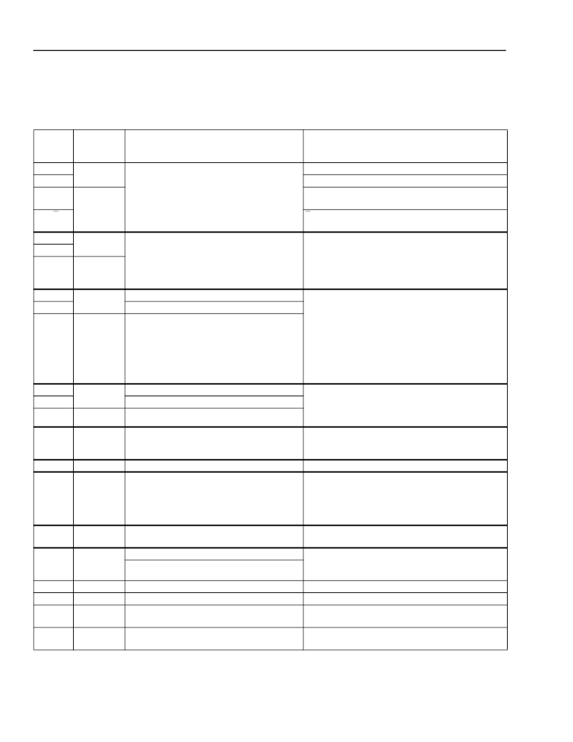
Table 131. Overall Replacement Table
Symbol
Used in
Instruction
Type(s)
F1, F2, F3,
F4
F1
Replaced By
Description
aD
aS
aT
a0
or
a1
(DSP16XX-compatible)
D
indicates
destination
of an operation.
S
indicates
source
of an operation.
T
indicates an accumulator that is the source of a data
transfer.
indicates an accumulator other than the destination
accumulator.
D
indicates
destination
of an operation.
S
indicates
source
of an operation.
T
indicates an accumulator
that is either an additional source for an operation or
the source or destination of a data transfer.
E
indi-
cates the
extended
set of accumulators.
a
aDE
aSE
aTE
F1E, F2E,
F3/E, F4/E
F1E, F3/E,
F4/E,
data move
F1E, F3E
a0
,
a1
,
a2
,
a3
,
a4
,
a5
,
a6
, or
a7
aDEE
aSEE
aTEE
a
DPE – 1
→
a0
,
a2
,
a4
, or
a6
a
SPE – 1
→
a0
,
a2
,
a4
, or
a6
a
TPE – 1
→
a0
,
a2
,
a4
, or
a6
D
indicates
destination
of an operation.
S
indicates
source
of an operation.
T
indicates an accumulator
that is either an additional source for an operation or
the source or destination of a data transfer. The first
E
indicates an
even
accumulator that is paired with its
corresponding paired extended (odd) accumulator,
i.e., the matching
aDPE
,
aSPE
, or
aTPE
accumulator.
The second
E
indicates the
extended
set of accumu-
lators.
P
indicates an odd accumulator that is
paired
with an
even extended accumulator, i.e., the matching
aDEE
,
aSEE
, or
aTEE
accumulator.
E
indicates the
extended
set of accumulators.
An accumulator vector, i.e., the concatenated 16-bit
high halves of two adjacent accumulators to form a
32-bit vector.
One of the four auxiliary accumulators.
Conditional mnemonics. Certain instructions are con-
ditionally executed, e.g.,
if CON F2E
. See
Table 134
on page 223
.
F3E
aDPE
aSPE
aTPE
F1E, F3E
a
DEE + 1
→
a1
,
a3
,
a5
, or
a7
a
SEE + 1
→
a1
,
a3
,
a5
, or
a7
a
TEE + 1
→
a1
,
a3
,
a5
, or
a7
F3E
aE_Ph
F1E
a0_1h
,
a2_3h
,
a4_5h
, or
a6_7h
arM
CON
F4, F4E
F1E, F2,
F2E, F3E,
F4E,
control,
data move
F3, F3E
ar0
,
ar1
,
ar2
, or
ar3
mi
,
pl
,
eq
,
ne
,
lvs
,
lvc
,
mvs
,
mvc
,
heads
,
tails
,
c0ge
,
c0lt
,
c1ge
,
c1lt
,
true
,
false
,
gt
,
le
,
oddp
,
evenp
,
smvs
,
smvc
,
jobf
,
jibe
,
jcont
,
lock
,
mgibe
,
mgobf
,
somef
,
somet
,
allf
, or
allt
max
,
min
, or
divs
FUNC
One of three ALU functions: maximum, minimum, or
divide-step.
Signed/unsigned status of the IM4 value matches that
of the destination register of the data move assign-
ment instruction.
Added to stack pointer
sp
to form stack address.
Vector for
icall
instruction.
Offset and width for bit-field insert and extract instruc-
tions. The BMU truncates these values to 6 bits.
Added to stack pointer
sp
to form stack address.
IM4
data move
4-bit unsigned immediate value (0 to 15)
4-bit signed immediate value (–8 to +7)
IM5
IM6
IM8O
IM8W
IM11
data move
control
F4
5-bit unsigned immediate value (0 to 31)
6-bit unsigned immediate value (0 to 63)
8-bit unsigned immediate value (0 to 255)
data move
11-bit unsigned immediate value
(0 to 2047)
The size of the transfer (single- or double-word) depends on the size of the register on the other side of the equal sign.
These postmodification options are not available for a double-word load except for a load of an accumulator vector.
D
D
相關PDF資料 |
PDF描述 |
|---|---|
| DSP16410 | 16-bit fixed point DSP with Flash |
| DSP25-16AR | Phase-leg Rectifier Diode |
| DSP25 | Phase-leg Rectifier Diode |
| DSP25-12A | Phase-leg Rectifier Diode |
| DSP25-12AT | Phase-leg Rectifier Diode |
相關代理商/技術參數(shù) |
參數(shù)描述 |
|---|---|
| DSP16410CG | 制造商:AGERE 制造商全稱:AGERE 功能描述:DSP16410CG Digital Signal Processor |
| DSP16411 | 制造商:AGERE 制造商全稱:AGERE 功能描述:DSP16411 Digital Signal Processor |
| DSP1643 | 制造商:未知廠家 制造商全稱:未知廠家 功能描述:Telecommunication IC |
| DSP1648C | 制造商:AGERE 制造商全稱:AGERE 功能描述:Host-Based Controller V.92 Modem Chip Set |
| DSP1675TV2RDD12VDB | 制造商:Agere Systems 功能描述: |
發(fā)布緊急采購,3分鐘左右您將得到回復。