- 您現(xiàn)在的位置:買賣IC網(wǎng) > PDF目錄376460 > XRT7245 (Exar Corporation) DS3 ATM User Network Interface(DS3異步傳輸模式用戶網(wǎng)絡(luò)接口) PDF資料下載
參數(shù)資料
| 型號(hào): | XRT7245 |
| 廠商: | Exar Corporation |
| 英文描述: | DS3 ATM User Network Interface(DS3異步傳輸模式用戶網(wǎng)絡(luò)接口) |
| 中文描述: | DS3自動(dòng)柜員機(jī)用戶網(wǎng)絡(luò)接口(DS3異步傳輸模式用戶網(wǎng)絡(luò)接口) |
| 文件頁數(shù): | 173/324頁 |
| 文件大?。?/td> | 4103K |
| 代理商: | XRT7245 |
第1頁第2頁第3頁第4頁第5頁第6頁第7頁第8頁第9頁第10頁第11頁第12頁第13頁第14頁第15頁第16頁第17頁第18頁第19頁第20頁第21頁第22頁第23頁第24頁第25頁第26頁第27頁第28頁第29頁第30頁第31頁第32頁第33頁第34頁第35頁第36頁第37頁第38頁第39頁第40頁第41頁第42頁第43頁第44頁第45頁第46頁第47頁第48頁第49頁第50頁第51頁第52頁第53頁第54頁第55頁第56頁第57頁第58頁第59頁第60頁第61頁第62頁第63頁第64頁第65頁第66頁第67頁第68頁第69頁第70頁第71頁第72頁第73頁第74頁第75頁第76頁第77頁第78頁第79頁第80頁第81頁第82頁第83頁第84頁第85頁第86頁第87頁第88頁第89頁第90頁第91頁第92頁第93頁第94頁第95頁第96頁第97頁第98頁第99頁第100頁第101頁第102頁第103頁第104頁第105頁第106頁第107頁第108頁第109頁第110頁第111頁第112頁第113頁第114頁第115頁第116頁第117頁第118頁第119頁第120頁第121頁第122頁第123頁第124頁第125頁第126頁第127頁第128頁第129頁第130頁第131頁第132頁第133頁第134頁第135頁第136頁第137頁第138頁第139頁第140頁第141頁第142頁第143頁第144頁第145頁第146頁第147頁第148頁第149頁第150頁第151頁第152頁第153頁第154頁第155頁第156頁第157頁第158頁第159頁第160頁第161頁第162頁第163頁第164頁第165頁第166頁第167頁第168頁第169頁第170頁第171頁第172頁當(dāng)前第173頁第174頁第175頁第176頁第177頁第178頁第179頁第180頁第181頁第182頁第183頁第184頁第185頁第186頁第187頁第188頁第189頁第190頁第191頁第192頁第193頁第194頁第195頁第196頁第197頁第198頁第199頁第200頁第201頁第202頁第203頁第204頁第205頁第206頁第207頁第208頁第209頁第210頁第211頁第212頁第213頁第214頁第215頁第216頁第217頁第218頁第219頁第220頁第221頁第222頁第223頁第224頁第225頁第226頁第227頁第228頁第229頁第230頁第231頁第232頁第233頁第234頁第235頁第236頁第237頁第238頁第239頁第240頁第241頁第242頁第243頁第244頁第245頁第246頁第247頁第248頁第249頁第250頁第251頁第252頁第253頁第254頁第255頁第256頁第257頁第258頁第259頁第260頁第261頁第262頁第263頁第264頁第265頁第266頁第267頁第268頁第269頁第270頁第271頁第272頁第273頁第274頁第275頁第276頁第277頁第278頁第279頁第280頁第281頁第282頁第283頁第284頁第285頁第286頁第287頁第288頁第289頁第290頁第291頁第292頁第293頁第294頁第295頁第296頁第297頁第298頁第299頁第300頁第301頁第302頁第303頁第304頁第305頁第306頁第307頁第308頁第309頁第310頁第311頁第312頁第313頁第314頁第315頁第316頁第317頁第318頁第319頁第320頁第321頁第322頁第323頁第324頁
á
PRELIMINARY
DS3 UNI FOR ATM
XRT7245
REV. 1.03
173
6.2.2.5
The Transmit Cell Processor provides for some
performance monitoring of the communication link
between the various UNIs, over the “ATM Switching
System”. This performance monitoring feature is re-
ferred to as the “Data Path Integrity Check”.
The Receive Cell Processor, or some equivalent entity,
within a UNI device, will (after performing HEC byte
verification) write a “Data Path Integrity Check” pattern
into each cell prior to its being read and processed by
the ATM Layer processor. This cell (with the “Data
Path Integrity Check” pattern) will be routed through
the ATM switch, and possibly throughout the Wide
Area Network (WAN); before arriving to the Transmit
UTOPIA Interface block of a given XRT7245 DS3
UNI. The Transmit Cell Processor will read in this cell
from the Tx FIFO, and will, prior to inserting a new
Data Path Integrity Check
HEC byte into the cell, read in the fifth octet from the
Tx FIFO and check it for a specific pattern or value.
The user can configure the Transmit Cell Processor
to check for either a constant “55h” pattern or an al-
ternating pattern of “55h” and “AAh” for each cell. The
user can also configure the Transmit Cell Processor
to generate an interrupt if a Data Path Integrity Test
fails. The user can accomplish all of this by writing
the appropriate data to the “Tx CP Control” Register
(Address = 60h). The bit format (with the relevant bit
fields shaded) of this register is shown below.
Note:
1. The “Data Path Integrity Check” feature is disabled
if the Transmit (and Receive) UTOPIA Interface
blocks have been configured to handle 52 byte cells.
2. This “Data Path Integrity Test” is only performed on
user cells. The Transmit Cell Processor does not
perform this test on OAM or Idle Cells.
The role that each of these “shaded” bit field plays is
presented below.
Bit 4—TDPChk Pat—Test Data Path Integrity
Check Pattern
The Transmit Cell Processor is always checking for a
specific pattern in the fifth octet of a user cell re-
trieved from the Tx FIFO. This “Read/Write” bit allows
the user to specify the octet pattern that the Transmit
Cell Processor should be checking for. The following
table relates the contents of this bit field to the octet
pattern expected by the Transmit Cell Processor.
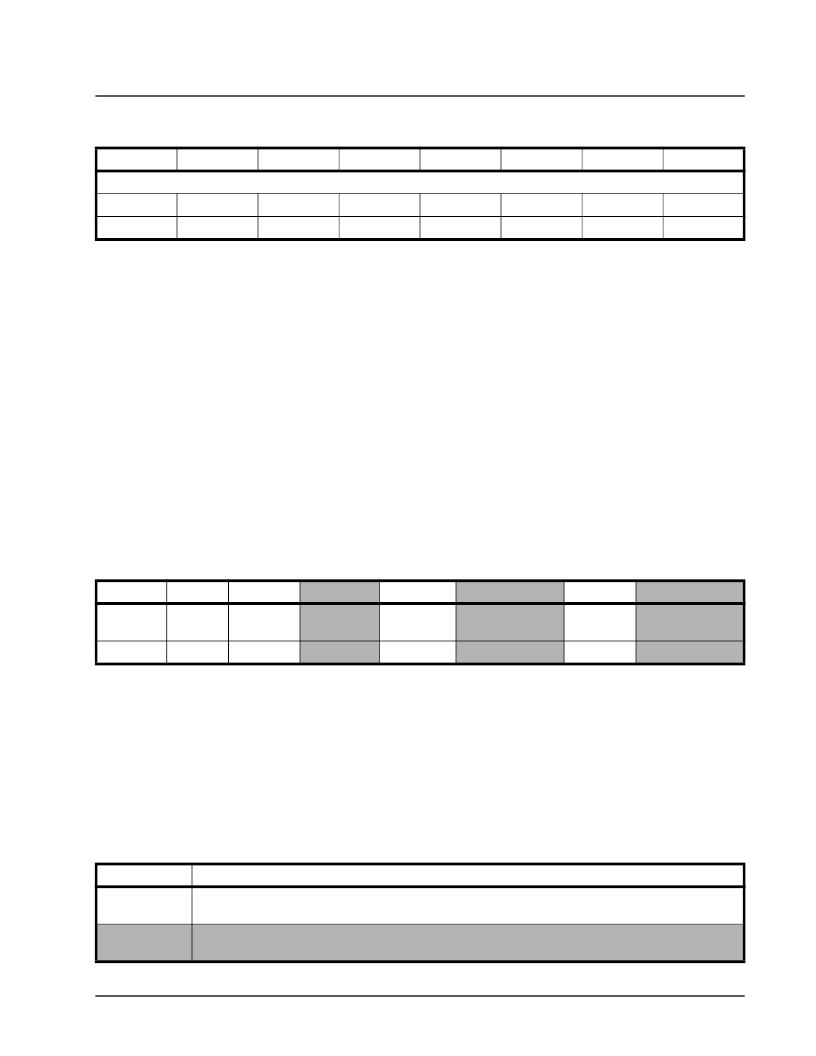
PMON Transmitted Idle Cell Count—LSB (Address = 39h)
B
IT
7
B
IT
6
B
IT
5
B
IT
4
B
IT
3
B
IT
2
B
IT
1
B
IT
0
Tx Idle Cell Count—Low Byte
RO
RO
RO
RO
RO
RO
RO
RO
0
0
0
0
0
0
0
0
Tx CP Control Register (Address = 60h)
B
IT
7
B
IT
6
B
IT
5
B
IT
4
B
IT
3
B
IT
2
B
IT
1
B
IT
0
Scrambler
Enable
Coset
Enable
HEC Insert
Enable
TDPChk
Pattern
GFC Insert
Enable
TDPErr Interrupt
Enable
Idle Cell
HEC CalEn
TDPErr Interrupt
Status
R/W
R/W
R/W
R/W
R/W
R/W
R/W
RUR
T
ABLE
20: T
HE
R
ELATIONSHIP
BETWEEN
THE
CONTENTS
OF
B
IT
4 (TDPC
HK
P
AT
)
WITHIN
THE
T
X
CP C
ONTROL
R
EGISTER
,
AND
THE
“D
ATA
P
ATH
I
NTEGRITY
C
HECK
” P
ATTERN
THAT
THE
T
RANSMIT
C
ELL
P
ROCESSOR
WILL
LOOK
FOR
IN
THE
5
TH
OCTET
OF
EACH
INCOMING
USER
CELL
TDPC
HK
P
AT
“D
ATA
P
ATH
I
NTEGRITY
P
ATTERN
” E
XPECTED
BY
THE
T
RANSMIT
C
ELL
P
ROCESSOR
0
Transmit Cell Processor expects an alternating “55h/AAh” pattern for the value of the fifth octet of the
cells received from the Tx FIFO.
1
Transmit Cell Processor expects a constant “55h” pattern for the value of the fifth octet of the cells
received from the Tx FIFO.
相關(guān)PDF資料 |
PDF描述 |
|---|---|
| XRT7288IP | CEPT1 Line Interface |
| XRT7288 | CEPT1 Line Interface(CEPT1線接口) |
| XRT7288IW | CEPT1 Line Interface |
| XRT7295AE | E3 (34.368Mbps) Integrated line Receiver |
| XRT7295AE_03 | E3 (34.368Mbps) Integrated line Receiver |
相關(guān)代理商/技術(shù)參數(shù) |
參數(shù)描述 |
|---|---|
| XRT7250 | 制造商:EXAR 制造商全稱:EXAR 功能描述:DS3/E3 FRAMER IC |
| XRT7250ES-PCI | 功能描述:界面開發(fā)工具 Evaluation Board for XRT7250 Series RoHS:否 制造商:Bourns 產(chǎn)品:Evaluation Boards 類型:RS-485 工具用于評(píng)估:ADM3485E 接口類型:RS-485 工作電源電壓:3.3 V |
| XRT7250IQ100 | 制造商:EXAR 制造商全稱:EXAR 功能描述:DS3/E3 FRAMER IC |
| XRT7288 | 制造商:EXAR 制造商全稱:EXAR 功能描述:CEPT1 Line Interface |
| XR-T7288 | 制造商:EXAR 制造商全稱:EXAR 功能描述:CEPT1 Line Interface |
發(fā)布緊急采購,3分鐘左右您將得到回復(fù)。