- 您現(xiàn)在的位置:買(mǎi)賣(mài)IC網(wǎng) > PDF目錄376460 > XRT7245 (Exar Corporation) DS3 ATM User Network Interface(DS3異步傳輸模式用戶(hù)網(wǎng)絡(luò)接口) PDF資料下載
參數(shù)資料
| 型號(hào): | XRT7245 |
| 廠(chǎng)商: | Exar Corporation |
| 英文描述: | DS3 ATM User Network Interface(DS3異步傳輸模式用戶(hù)網(wǎng)絡(luò)接口) |
| 中文描述: | DS3自動(dòng)柜員機(jī)用戶(hù)網(wǎng)絡(luò)接口(DS3異步傳輸模式用戶(hù)網(wǎng)絡(luò)接口) |
| 文件頁(yè)數(shù): | 170/324頁(yè) |
| 文件大小: | 4103K |
| 代理商: | XRT7245 |
第1頁(yè)第2頁(yè)第3頁(yè)第4頁(yè)第5頁(yè)第6頁(yè)第7頁(yè)第8頁(yè)第9頁(yè)第10頁(yè)第11頁(yè)第12頁(yè)第13頁(yè)第14頁(yè)第15頁(yè)第16頁(yè)第17頁(yè)第18頁(yè)第19頁(yè)第20頁(yè)第21頁(yè)第22頁(yè)第23頁(yè)第24頁(yè)第25頁(yè)第26頁(yè)第27頁(yè)第28頁(yè)第29頁(yè)第30頁(yè)第31頁(yè)第32頁(yè)第33頁(yè)第34頁(yè)第35頁(yè)第36頁(yè)第37頁(yè)第38頁(yè)第39頁(yè)第40頁(yè)第41頁(yè)第42頁(yè)第43頁(yè)第44頁(yè)第45頁(yè)第46頁(yè)第47頁(yè)第48頁(yè)第49頁(yè)第50頁(yè)第51頁(yè)第52頁(yè)第53頁(yè)第54頁(yè)第55頁(yè)第56頁(yè)第57頁(yè)第58頁(yè)第59頁(yè)第60頁(yè)第61頁(yè)第62頁(yè)第63頁(yè)第64頁(yè)第65頁(yè)第66頁(yè)第67頁(yè)第68頁(yè)第69頁(yè)第70頁(yè)第71頁(yè)第72頁(yè)第73頁(yè)第74頁(yè)第75頁(yè)第76頁(yè)第77頁(yè)第78頁(yè)第79頁(yè)第80頁(yè)第81頁(yè)第82頁(yè)第83頁(yè)第84頁(yè)第85頁(yè)第86頁(yè)第87頁(yè)第88頁(yè)第89頁(yè)第90頁(yè)第91頁(yè)第92頁(yè)第93頁(yè)第94頁(yè)第95頁(yè)第96頁(yè)第97頁(yè)第98頁(yè)第99頁(yè)第100頁(yè)第101頁(yè)第102頁(yè)第103頁(yè)第104頁(yè)第105頁(yè)第106頁(yè)第107頁(yè)第108頁(yè)第109頁(yè)第110頁(yè)第111頁(yè)第112頁(yè)第113頁(yè)第114頁(yè)第115頁(yè)第116頁(yè)第117頁(yè)第118頁(yè)第119頁(yè)第120頁(yè)第121頁(yè)第122頁(yè)第123頁(yè)第124頁(yè)第125頁(yè)第126頁(yè)第127頁(yè)第128頁(yè)第129頁(yè)第130頁(yè)第131頁(yè)第132頁(yè)第133頁(yè)第134頁(yè)第135頁(yè)第136頁(yè)第137頁(yè)第138頁(yè)第139頁(yè)第140頁(yè)第141頁(yè)第142頁(yè)第143頁(yè)第144頁(yè)第145頁(yè)第146頁(yè)第147頁(yè)第148頁(yè)第149頁(yè)第150頁(yè)第151頁(yè)第152頁(yè)第153頁(yè)第154頁(yè)第155頁(yè)第156頁(yè)第157頁(yè)第158頁(yè)第159頁(yè)第160頁(yè)第161頁(yè)第162頁(yè)第163頁(yè)第164頁(yè)第165頁(yè)第166頁(yè)第167頁(yè)第168頁(yè)第169頁(yè)當(dāng)前第170頁(yè)第171頁(yè)第172頁(yè)第173頁(yè)第174頁(yè)第175頁(yè)第176頁(yè)第177頁(yè)第178頁(yè)第179頁(yè)第180頁(yè)第181頁(yè)第182頁(yè)第183頁(yè)第184頁(yè)第185頁(yè)第186頁(yè)第187頁(yè)第188頁(yè)第189頁(yè)第190頁(yè)第191頁(yè)第192頁(yè)第193頁(yè)第194頁(yè)第195頁(yè)第196頁(yè)第197頁(yè)第198頁(yè)第199頁(yè)第200頁(yè)第201頁(yè)第202頁(yè)第203頁(yè)第204頁(yè)第205頁(yè)第206頁(yè)第207頁(yè)第208頁(yè)第209頁(yè)第210頁(yè)第211頁(yè)第212頁(yè)第213頁(yè)第214頁(yè)第215頁(yè)第216頁(yè)第217頁(yè)第218頁(yè)第219頁(yè)第220頁(yè)第221頁(yè)第222頁(yè)第223頁(yè)第224頁(yè)第225頁(yè)第226頁(yè)第227頁(yè)第228頁(yè)第229頁(yè)第230頁(yè)第231頁(yè)第232頁(yè)第233頁(yè)第234頁(yè)第235頁(yè)第236頁(yè)第237頁(yè)第238頁(yè)第239頁(yè)第240頁(yè)第241頁(yè)第242頁(yè)第243頁(yè)第244頁(yè)第245頁(yè)第246頁(yè)第247頁(yè)第248頁(yè)第249頁(yè)第250頁(yè)第251頁(yè)第252頁(yè)第253頁(yè)第254頁(yè)第255頁(yè)第256頁(yè)第257頁(yè)第258頁(yè)第259頁(yè)第260頁(yè)第261頁(yè)第262頁(yè)第263頁(yè)第264頁(yè)第265頁(yè)第266頁(yè)第267頁(yè)第268頁(yè)第269頁(yè)第270頁(yè)第271頁(yè)第272頁(yè)第273頁(yè)第274頁(yè)第275頁(yè)第276頁(yè)第277頁(yè)第278頁(yè)第279頁(yè)第280頁(yè)第281頁(yè)第282頁(yè)第283頁(yè)第284頁(yè)第285頁(yè)第286頁(yè)第287頁(yè)第288頁(yè)第289頁(yè)第290頁(yè)第291頁(yè)第292頁(yè)第293頁(yè)第294頁(yè)第295頁(yè)第296頁(yè)第297頁(yè)第298頁(yè)第299頁(yè)第300頁(yè)第301頁(yè)第302頁(yè)第303頁(yè)第304頁(yè)第305頁(yè)第306頁(yè)第307頁(yè)第308頁(yè)第309頁(yè)第310頁(yè)第311頁(yè)第312頁(yè)第313頁(yè)第314頁(yè)第315頁(yè)第316頁(yè)第317頁(yè)第318頁(yè)第319頁(yè)第320頁(yè)第321頁(yè)第322頁(yè)第323頁(yè)第324頁(yè)
XRT7245
DS3 UNI FOR ATM
á
PRELIMINARY
REV. 1.03
170
A “1” in this bit-field enables the Cell Scrambler. Con-
versely, a “0” in this bit-field disables the Cell-Scrambler.
Upon power up or reset, the Cell Scrambler function
will be enabled. Therefore, the user must write a “0”
to this bit in order to disable cell scrambling.
6.2.2.3
The first four bits in the first header byte of each cell
are allocated for carrying “Generic Flow Control” (GFC)
GFC Nibble-Field Serial Input Port
information. The user can externally insert his/her own
values for the GFC nibble-field into each outbound
cell, via a serial input port. The user will activate this
serial input port (the “Transmit GFC-Nibble-field” Serial
Input port) by writing a “1” to bit 3 (GFC Insert Enable)
of the “TxCP Control” Register, as depicted below.
Once the user has activated the “Transmit GFC Nibble-
field” Serial input port, it will accept the 4 bit GFC val-
ue via the TxGFC pin during each cell processing pe-
riod. The TxGFC serial input port will be expecting
the bits of the GFC nibble-field in descending order
(MSB first). The GFC bits are clocked into the serial
input port via the rising edge of the clock signal,
TxG-FCClk. Since these four bits must be provided
for each cell; TxGFCClk will provide four clock edges
during each cell processing period. The “Transmit
GFC Nibble-field” Serial input port will also provide a
“framing pulse” in the form of the TxGFCMSB output
pin pulsing “high”. This output pin will pulse “high”
when the Transmit Cell Processor is ready to receive
the MSB (most significant bit) of the GFC field.
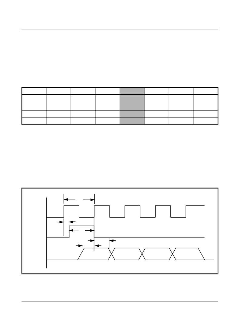
Figure 45 presents a timing diagram illustrating the
role of each of these signals during GFC insertion.
6.2.2.4 OAM Cell Processing
The UNI chip provides on-chip RAM space for the
storage of the complete contents (header and pay-
load) of an OAM cell. This RAM space is known as
the “Transmit OAM Cell” buffer (consisting of 54
bytes) and is located at 136h through 16Bh in the
UNI address space. Therefore, in order to “l(fā)oad” the
TxCP Control Register (Address = 60h)
B
IT
7
B
IT
6
B
IT
5
B
IT
4
B
IT
3
B
IT
2
B
IT
1
B
IT
0
Scrambler
Enable
Coset
Enable
HEC Insert
Enable
TDPChk
Pattern
GFC Insert
Enable
TDPErr
Interrupt
Enable
Idle Cell
HEC CalEn
TDPErr
Interrupt
Status
R/W
R/W
R/W
R/W
R/W
R/W
R/W
RUR
1
1
1
1
x
0
1
0
F
IGURE
45. B
EHAVIOR
OF
T
X
GFC, T
X
GFCC
LK
,
AND
T
X
GFCMSB
DURING
GFC
INSERTION
INTO
THE
“O
UTBOUND
” C
ELL
TxGFCClk
TxGFCMSB
t14
TxGFC
t16
BIT 3
BIT 2
BIT 1
BIT 0
t17
t13
t15
相關(guān)PDF資料 |
PDF描述 |
|---|---|
| XRT7288IP | CEPT1 Line Interface |
| XRT7288 | CEPT1 Line Interface(CEPT1線(xiàn)接口) |
| XRT7288IW | CEPT1 Line Interface |
| XRT7295AE | E3 (34.368Mbps) Integrated line Receiver |
| XRT7295AE_03 | E3 (34.368Mbps) Integrated line Receiver |
相關(guān)代理商/技術(shù)參數(shù) |
參數(shù)描述 |
|---|---|
| XRT7250 | 制造商:EXAR 制造商全稱(chēng):EXAR 功能描述:DS3/E3 FRAMER IC |
| XRT7250ES-PCI | 功能描述:界面開(kāi)發(fā)工具 Evaluation Board for XRT7250 Series RoHS:否 制造商:Bourns 產(chǎn)品:Evaluation Boards 類(lèi)型:RS-485 工具用于評(píng)估:ADM3485E 接口類(lèi)型:RS-485 工作電源電壓:3.3 V |
| XRT7250IQ100 | 制造商:EXAR 制造商全稱(chēng):EXAR 功能描述:DS3/E3 FRAMER IC |
| XRT7288 | 制造商:EXAR 制造商全稱(chēng):EXAR 功能描述:CEPT1 Line Interface |
| XR-T7288 | 制造商:EXAR 制造商全稱(chēng):EXAR 功能描述:CEPT1 Line Interface |
發(fā)布緊急采購(gòu),3分鐘左右您將得到回復(fù)。