- 您現(xiàn)在的位置:買賣IC網(wǎng) > PDF目錄376460 > XRT7245 (Exar Corporation) DS3 ATM User Network Interface(DS3異步傳輸模式用戶網(wǎng)絡(luò)接口) PDF資料下載
參數(shù)資料
| 型號: | XRT7245 |
| 廠商: | Exar Corporation |
| 英文描述: | DS3 ATM User Network Interface(DS3異步傳輸模式用戶網(wǎng)絡(luò)接口) |
| 中文描述: | DS3自動柜員機(jī)用戶網(wǎng)絡(luò)接口(DS3異步傳輸模式用戶網(wǎng)絡(luò)接口) |
| 文件頁數(shù): | 118/324頁 |
| 文件大小: | 4103K |
| 代理商: | XRT7245 |
第1頁第2頁第3頁第4頁第5頁第6頁第7頁第8頁第9頁第10頁第11頁第12頁第13頁第14頁第15頁第16頁第17頁第18頁第19頁第20頁第21頁第22頁第23頁第24頁第25頁第26頁第27頁第28頁第29頁第30頁第31頁第32頁第33頁第34頁第35頁第36頁第37頁第38頁第39頁第40頁第41頁第42頁第43頁第44頁第45頁第46頁第47頁第48頁第49頁第50頁第51頁第52頁第53頁第54頁第55頁第56頁第57頁第58頁第59頁第60頁第61頁第62頁第63頁第64頁第65頁第66頁第67頁第68頁第69頁第70頁第71頁第72頁第73頁第74頁第75頁第76頁第77頁第78頁第79頁第80頁第81頁第82頁第83頁第84頁第85頁第86頁第87頁第88頁第89頁第90頁第91頁第92頁第93頁第94頁第95頁第96頁第97頁第98頁第99頁第100頁第101頁第102頁第103頁第104頁第105頁第106頁第107頁第108頁第109頁第110頁第111頁第112頁第113頁第114頁第115頁第116頁第117頁當(dāng)前第118頁第119頁第120頁第121頁第122頁第123頁第124頁第125頁第126頁第127頁第128頁第129頁第130頁第131頁第132頁第133頁第134頁第135頁第136頁第137頁第138頁第139頁第140頁第141頁第142頁第143頁第144頁第145頁第146頁第147頁第148頁第149頁第150頁第151頁第152頁第153頁第154頁第155頁第156頁第157頁第158頁第159頁第160頁第161頁第162頁第163頁第164頁第165頁第166頁第167頁第168頁第169頁第170頁第171頁第172頁第173頁第174頁第175頁第176頁第177頁第178頁第179頁第180頁第181頁第182頁第183頁第184頁第185頁第186頁第187頁第188頁第189頁第190頁第191頁第192頁第193頁第194頁第195頁第196頁第197頁第198頁第199頁第200頁第201頁第202頁第203頁第204頁第205頁第206頁第207頁第208頁第209頁第210頁第211頁第212頁第213頁第214頁第215頁第216頁第217頁第218頁第219頁第220頁第221頁第222頁第223頁第224頁第225頁第226頁第227頁第228頁第229頁第230頁第231頁第232頁第233頁第234頁第235頁第236頁第237頁第238頁第239頁第240頁第241頁第242頁第243頁第244頁第245頁第246頁第247頁第248頁第249頁第250頁第251頁第252頁第253頁第254頁第255頁第256頁第257頁第258頁第259頁第260頁第261頁第262頁第263頁第264頁第265頁第266頁第267頁第268頁第269頁第270頁第271頁第272頁第273頁第274頁第275頁第276頁第277頁第278頁第279頁第280頁第281頁第282頁第283頁第284頁第285頁第286頁第287頁第288頁第289頁第290頁第291頁第292頁第293頁第294頁第295頁第296頁第297頁第298頁第299頁第300頁第301頁第302頁第303頁第304頁第305頁第306頁第307頁第308頁第309頁第310頁第311頁第312頁第313頁第314頁第315頁第316頁第317頁第318頁第319頁第320頁第321頁第322頁第323頁第324頁
XRT7245
DS3 UNI FOR ATM
á
PRELIMINARY
REV. 1.03
118
3.3.2.116
PMON CP Bit Error Count Register (MSB)
This “Reset-upon-Read” register, along with the “PMON
CP Bit Error Count—LSB” register (Address = 75h)
contains a 16 bit representation of the number of CP
Bit Errors that have been detected by the Receive
DS3 Framer, since the last read of these register.
This register contains the MSB (or Upper Byte) value
of this 16-bit expression.
3.4
The “Loss of Clock Enable” Feature
The timing for the Microprocessor Interface section
originates from a 44.736 MHz signal that is provided
by either the TxInClk or the RxLineClk signals. How-
ever, if the UNI device experiences a “Loss of Clock
signal” event such that neither the TxInClk nor the
RxLineClk signal are present, then the UNI Micropro-
cessor Interface section ceases to function.
The UNI device offers a “Loss of Clock” (LOC) protec-
tion feature that allows the Microprocessor Interface
section to at least complete or terminate an “in-process”
Read or Write cycle (with the local μP) should this
“Loss of Clock” event occur. The “LOC” circuitry
consists of a ring oscillator that continuously checks
for signal transitions at the TxInClk and RxLineClk
input pins. If a “Loss of Clock Signal” event occurs
such that no transitions are occurring on these pins,
then the LOC circuitry will automatically assert the
Rdy_Dtck signal in order to complete (or terminate)
the current “Read” or “Write” cycle with the UNI
Microprocessor Interface section.
The user may enable or disable this “LOC Protection”
feature by writing to Bit 7 (LOC Enable) within the
UNI I/O Register, as depicted below.
Writing a “1” to this bit-field enables this “LOC
Protection” feature. Writing a “0” to this bit-field
disables this feature.
Note:
The “Ring Oscillator” can be a source of noise,
within the UNI chip. Hence, there may be situations where
the user will wish to disable the “LOC Protection” feature.
3.5
Using the PMON Holding Register
If the Microprocessor Interface section is configured
to operate over an 8-bit data bus, then the local μP
will be able to read from and write to the UNI on-chip
registers, 8 bit per (read or write) cycle. Since most of
the UNI on-chip registers contain 8-bits, communicating
with the local μP over an 8-bit data bus, is not much of
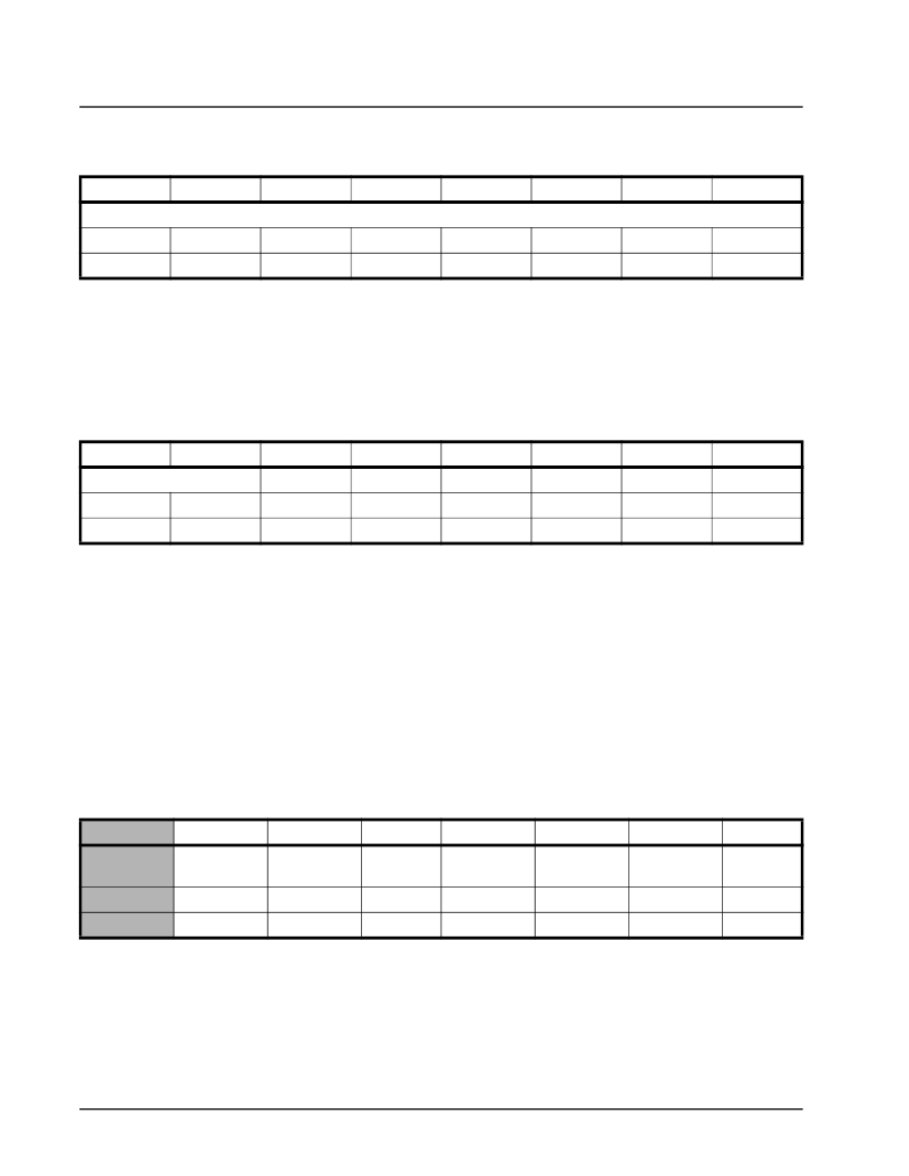
Address = 74h, PMON CP Bit Error Count—MSB
B
IT
7
B
IT
6
B
IT
5
B
IT
4
B
IT
3
B
IT
2
B
IT
1
B
IT
0
Rx CP Bit Error Count—Upper Byte
RUR
RUR
RUR
RUR
RUR
RUR
RUR
RUR
0
0
0
0
0
0
0
0
Address = 72h, Line Interface Drive Register
B
IT
7
B
IT
6
B
IT
5
B
IT
4
B
IT
3
B
IT
2
B
IT
1
B
IT
0
Unused
REQB
TAOS
Encodis
TxLev
RLoop
LLoop
RO
RO
R/W
R/W
R/W
R/W
R/W
R/W
0
0
0
0
0
0
0
0
Address = 01h, UNI I/O Control Register
B
IT
7
B
IT
6
B
IT
5
B
IT
4
B
IT
3
B
IT
2
B
IT
1
B
IT
0
LOC Enable
Test
PMON
Interrupt
Enable Reset
AMI/B3ZS*
Unipolar/
Bipolar*
TxLine
Clk Inv
RxLine
Clk Inv
Reframe
R/W
R/W
R/W
R/W
R/W
R/W
R/W
R/W
0
0
0
0
0
0
0
0
相關(guān)PDF資料 |
PDF描述 |
|---|---|
| XRT7288IP | CEPT1 Line Interface |
| XRT7288 | CEPT1 Line Interface(CEPT1線接口) |
| XRT7288IW | CEPT1 Line Interface |
| XRT7295AE | E3 (34.368Mbps) Integrated line Receiver |
| XRT7295AE_03 | E3 (34.368Mbps) Integrated line Receiver |
相關(guān)代理商/技術(shù)參數(shù) |
參數(shù)描述 |
|---|---|
| XRT7250 | 制造商:EXAR 制造商全稱:EXAR 功能描述:DS3/E3 FRAMER IC |
| XRT7250ES-PCI | 功能描述:界面開發(fā)工具 Evaluation Board for XRT7250 Series RoHS:否 制造商:Bourns 產(chǎn)品:Evaluation Boards 類型:RS-485 工具用于評估:ADM3485E 接口類型:RS-485 工作電源電壓:3.3 V |
| XRT7250IQ100 | 制造商:EXAR 制造商全稱:EXAR 功能描述:DS3/E3 FRAMER IC |
| XRT7288 | 制造商:EXAR 制造商全稱:EXAR 功能描述:CEPT1 Line Interface |
| XR-T7288 | 制造商:EXAR 制造商全稱:EXAR 功能描述:CEPT1 Line Interface |
發(fā)布緊急采購,3分鐘左右您將得到回復(fù)。