- 您現(xiàn)在的位置:買賣IC網(wǎng) > PDF目錄377000 > DSP16210 TVS 400W 6.5V UNIDIRECT SMA PDF資料下載
參數(shù)資料
| 型號: | DSP16210 |
| 英文描述: | TVS 400W 6.5V UNIDIRECT SMA |
| 中文描述: | DSP16210數(shù)字信號處理器 |
| 文件頁數(shù): | 37/173頁 |
| 文件大?。?/td> | 2621K |
| 代理商: | DSP16210 |
第1頁第2頁第3頁第4頁第5頁第6頁第7頁第8頁第9頁第10頁第11頁第12頁第13頁第14頁第15頁第16頁第17頁第18頁第19頁第20頁第21頁第22頁第23頁第24頁第25頁第26頁第27頁第28頁第29頁第30頁第31頁第32頁第33頁第34頁第35頁第36頁當前第37頁第38頁第39頁第40頁第41頁第42頁第43頁第44頁第45頁第46頁第47頁第48頁第49頁第50頁第51頁第52頁第53頁第54頁第55頁第56頁第57頁第58頁第59頁第60頁第61頁第62頁第63頁第64頁第65頁第66頁第67頁第68頁第69頁第70頁第71頁第72頁第73頁第74頁第75頁第76頁第77頁第78頁第79頁第80頁第81頁第82頁第83頁第84頁第85頁第86頁第87頁第88頁第89頁第90頁第91頁第92頁第93頁第94頁第95頁第96頁第97頁第98頁第99頁第100頁第101頁第102頁第103頁第104頁第105頁第106頁第107頁第108頁第109頁第110頁第111頁第112頁第113頁第114頁第115頁第116頁第117頁第118頁第119頁第120頁第121頁第122頁第123頁第124頁第125頁第126頁第127頁第128頁第129頁第130頁第131頁第132頁第133頁第134頁第135頁第136頁第137頁第138頁第139頁第140頁第141頁第142頁第143頁第144頁第145頁第146頁第147頁第148頁第149頁第150頁第151頁第152頁第153頁第154頁第155頁第156頁第157頁第158頁第159頁第160頁第161頁第162頁第163頁第164頁第165頁第166頁第167頁第168頁第169頁第170頁第171頁第172頁第173頁
Data Sheet
July 2000
DSP16210 Digital Signal Processor
Lucent Technologies Inc.
DRAFT COPY
37
Hardware Architecture
(continued)
Enhanced Serial I/O Unit (ESIO)
(continued)
OCR
(
Table 59 on page 102
) controls the configuration
of the output section, including the selection of simple
mode vs. frame mode.
OCVV
(
Table 62 on page 103
)
specifies the number of active logical channels (one for
simple mode and 1 through 16 for frame mode).
OCSB
0—7
(
Table 60 on page 103
) and
OCSL
0—1
(
Table 61 on page 103
) are used only in frame mode.
They specify the starting bit position and the sample
length (1, 2, 4, or 8 bits) of each logical channel.
As illustrated in Figure 12, OLEV (bit 3) of the
OCR
register selects the polarity of the output bit clock,
EOBC. This modified clock is the output bit clock for
the output section (OBC). OSLEV (bit 8) of the
OCR
register selects whether or not the output frame sync,
EOFS, is inverted. This modified signal is the frame
sync for the output section (OFS).
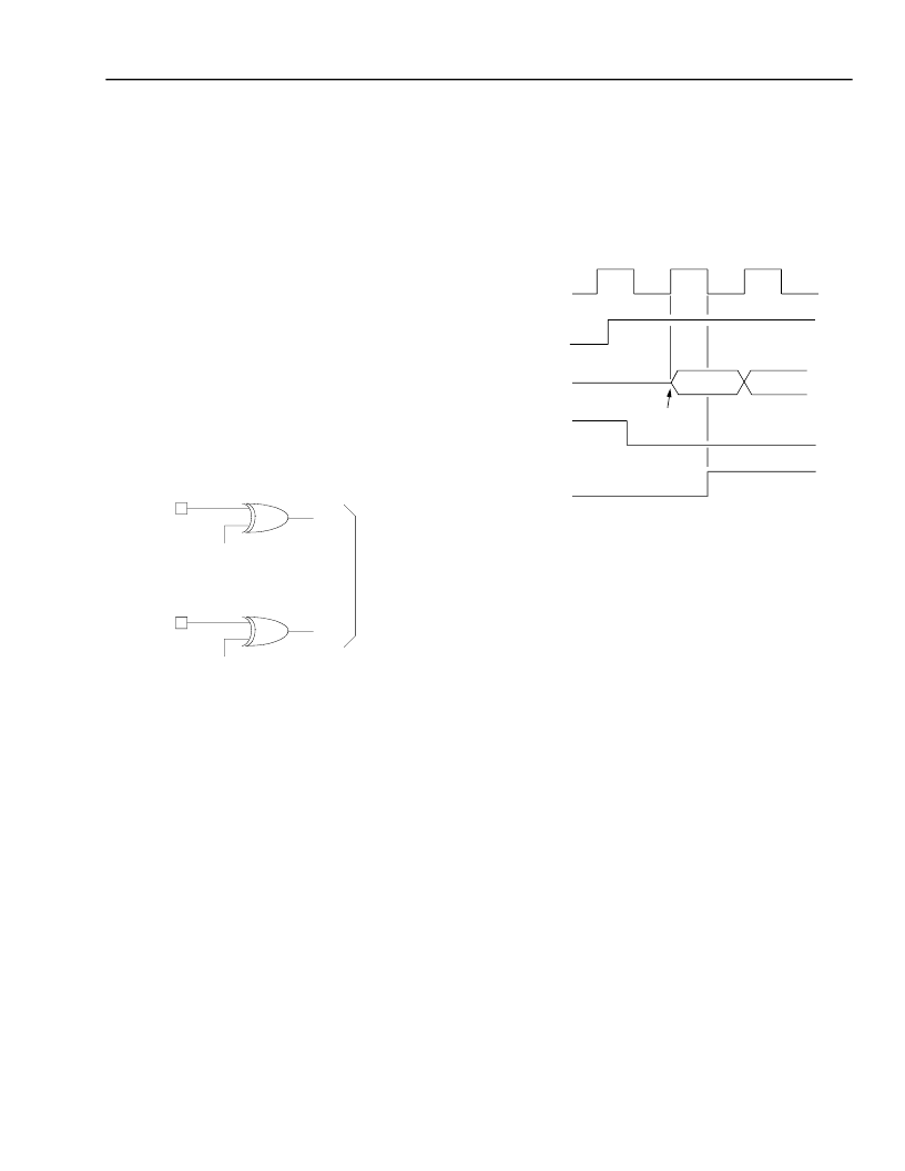
Figure 12. Output Control Signal Conditioning
As illustrated in
Figure 13
, the ESIO drives serial data
onto the ESIO data out (EDO) pin the rising edge of the
output bit clock (OBC). The rising edge of output frame
sync (OFS) indicates that the first bit of the serial out-
put packet or frame is driven onto EDO on the next ris-
ing edge of OBC. This edge (as captured by OBC) also
initializes the internal bit counter to zero, and every
subsequent rising edge of OBC increments the bit
counter. In frame mode, this bit counter is used by the
output control hardware to define logical channel start
points and to detect output frame errors.
The ESIO asserts the EOBE output pin and the EOBE
interrupt on the falling edge of OBC following detection
of OFS as shown in
Figure 13
. EOBE is cleared when
the DSP program writes any of the
OMX
0—15
mem-
ory-mapped registers. EOBE is also cleared on device
reset or if the DSP program resets the output section
by writing the
OCR
register with the ORESET field
(bit 4) set.
Figure 13. Output Functional Timing
The ESIO drives EDO only during its scheduled
timeslot as illustrated in
Figure 13
. Otherwise EDO is in
the high-impedance state. The other necessary condi-
tions for the DSP16210 to drive EDO are:
I
The EOEB negative-assertion input pin must be
asserted (low).
I
The EDOEO bit in the
OCR
register (bit 6) must be
set.
If EOEB is high or if the EDOEO bit is cleared, then
EDO is in the high-impedance state regardless of the
state of ESIO output section. The EDOEO bit is cleared
on reset causing the EDO pin to be in the high-imped-
ance state by default.
The EDOMD bit in
OCR
(bit 5) configures the EDO out-
put pin driver as either 3-state or open-drain.
EOFS
EOBC
OFS
OBC
FRAME SYNC
AND
CLOCK
FOR
ESIO
OUTPUT
SECTION
OSLEV
(OCR[8])
OLEV
(OCR[3])
OBC
OFS
EDO
B
0
B
1
INTERNAL
BIT COUNTER
CLEARED
EOEB
EOBE
相關PDF資料 |
PDF描述 |
|---|---|
| DSP1627 | TVS 400W 6.5V BIDIRECT SMA |
| DSP1629 | TVS 400W 64V UNIDIRECT SMA |
| DSP16410C | TVS 400W 7.0V UNIDIRECT SMA |
| DSP16410 | 16-bit fixed point DSP with Flash |
| DSP25-16AR | Phase-leg Rectifier Diode |
相關代理商/技術參數(shù) |
參數(shù)描述 |
|---|---|
| DSP1627 | 制造商:AGERE 制造商全稱:AGERE 功能描述:DSP1627 Digital Signal Processor |
| DSP1627F32K10IR | 制造商:未知廠家 制造商全稱:未知廠家 功能描述:DSP|16-BIT|CMOS|QFP|100PIN|PLASTIC |
| DSP1627F32K10IT | 制造商:未知廠家 制造商全稱:未知廠家 功能描述:DSP|16-BIT|CMOS|QFP|100PIN|PLASTIC |
| DSP1627F32K11I | 制造商:未知廠家 制造商全稱:未知廠家 功能描述:16-Bit Digital Signal Processor |
| DSP1627F32K11IR | 制造商:未知廠家 制造商全稱:未知廠家 功能描述:DSP|16-BIT|CMOS|QFP|100PIN|PLASTIC |
發(fā)布緊急采購,3分鐘左右您將得到回復。