- 您現(xiàn)在的位置:買賣IC網(wǎng) > PDF目錄370261 > FW82815 Controller Miscellaneous - Datasheet Reference PDF資料下載
參數(shù)資料
| 型號(hào): | FW82815 |
| 英文描述: | Controller Miscellaneous - Datasheet Reference |
| 中文描述: | 控制器雜項(xiàng)-數(shù)據(jù)表參考 |
| 文件頁(yè)數(shù): | 31/172頁(yè) |
| 文件大?。?/td> | 795K |
| 代理商: | FW82815 |
第1頁(yè)第2頁(yè)第3頁(yè)第4頁(yè)第5頁(yè)第6頁(yè)第7頁(yè)第8頁(yè)第9頁(yè)第10頁(yè)第11頁(yè)第12頁(yè)第13頁(yè)第14頁(yè)第15頁(yè)第16頁(yè)第17頁(yè)第18頁(yè)第19頁(yè)第20頁(yè)第21頁(yè)第22頁(yè)第23頁(yè)第24頁(yè)第25頁(yè)第26頁(yè)第27頁(yè)第28頁(yè)第29頁(yè)第30頁(yè)當(dāng)前第31頁(yè)第32頁(yè)第33頁(yè)第34頁(yè)第35頁(yè)第36頁(yè)第37頁(yè)第38頁(yè)第39頁(yè)第40頁(yè)第41頁(yè)第42頁(yè)第43頁(yè)第44頁(yè)第45頁(yè)第46頁(yè)第47頁(yè)第48頁(yè)第49頁(yè)第50頁(yè)第51頁(yè)第52頁(yè)第53頁(yè)第54頁(yè)第55頁(yè)第56頁(yè)第57頁(yè)第58頁(yè)第59頁(yè)第60頁(yè)第61頁(yè)第62頁(yè)第63頁(yè)第64頁(yè)第65頁(yè)第66頁(yè)第67頁(yè)第68頁(yè)第69頁(yè)第70頁(yè)第71頁(yè)第72頁(yè)第73頁(yè)第74頁(yè)第75頁(yè)第76頁(yè)第77頁(yè)第78頁(yè)第79頁(yè)第80頁(yè)第81頁(yè)第82頁(yè)第83頁(yè)第84頁(yè)第85頁(yè)第86頁(yè)第87頁(yè)第88頁(yè)第89頁(yè)第90頁(yè)第91頁(yè)第92頁(yè)第93頁(yè)第94頁(yè)第95頁(yè)第96頁(yè)第97頁(yè)第98頁(yè)第99頁(yè)第100頁(yè)第101頁(yè)第102頁(yè)第103頁(yè)第104頁(yè)第105頁(yè)第106頁(yè)第107頁(yè)第108頁(yè)第109頁(yè)第110頁(yè)第111頁(yè)第112頁(yè)第113頁(yè)第114頁(yè)第115頁(yè)第116頁(yè)第117頁(yè)第118頁(yè)第119頁(yè)第120頁(yè)第121頁(yè)第122頁(yè)第123頁(yè)第124頁(yè)第125頁(yè)第126頁(yè)第127頁(yè)第128頁(yè)第129頁(yè)第130頁(yè)第131頁(yè)第132頁(yè)第133頁(yè)第134頁(yè)第135頁(yè)第136頁(yè)第137頁(yè)第138頁(yè)第139頁(yè)第140頁(yè)第141頁(yè)第142頁(yè)第143頁(yè)第144頁(yè)第145頁(yè)第146頁(yè)第147頁(yè)第148頁(yè)第149頁(yè)第150頁(yè)第151頁(yè)第152頁(yè)第153頁(yè)第154頁(yè)第155頁(yè)第156頁(yè)第157頁(yè)第158頁(yè)第159頁(yè)第160頁(yè)第161頁(yè)第162頁(yè)第163頁(yè)第164頁(yè)第165頁(yè)第166頁(yè)第167頁(yè)第168頁(yè)第169頁(yè)第170頁(yè)第171頁(yè)第172頁(yè)
82815 GMCH
R
Datasheet
31
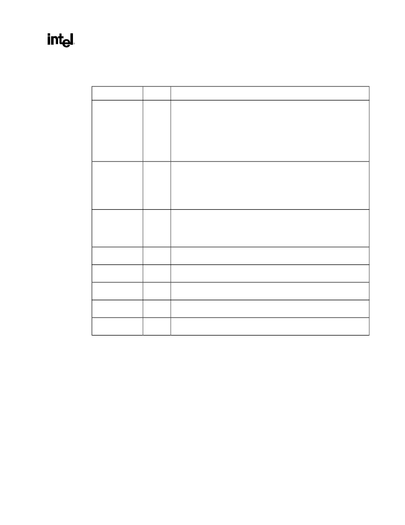
2.7.
Digital Video Output Signals/TV-Out Pins
Signal Name
Type
Description
TVCLKIN/INT#
I
1.8V
Low Voltage TV Clock In (TV-Out Mode).
In 1.8V TV-Out usage, the TVCLKIN
pin functions as a pixel clock input to the GMCH from the TV encoder. The
TVCLKIN frequency ranges from 20 MHz to 40 MHz depending on the mode
(e.g., NTSC or PAL) and the overscan compensation values in the TV Encoder.
CLKIN has a worse case duty cycle of 60%/40% coming in to the GMCH.
Flat Panel Interrupt (LCD Mode).
In Flat Panel usage, the INT# pin is asserted
to cause an interrupt (typically, to indicate a hot plug or unplug of a flat panel). In
Flat Panel usage, this pin is connected internally to a pull-up resistor.
LTVCLKOUT[1:0]
O
1.8V
LCD/TV Port Clock Out:
These pins provide a differential pair reference clock
that can run up to 85 MHz.
Note:
It is always recommended that these pins be used as a differential pair.
Devices running at frequencies less than 65 MHz can operate in single-ended
clock mode and use LTVCLKOUT[0] as the clock. When operating in single-
ended clock mode, LTVCLKOUT[1] is not used.
LTVBLANK#
O
1.8V
Flicker Blank or Border Period Indication.
BLANK# is a programmable output
pin driven by the graphics control. When programmed as a blank period
indication, this pin indicates active pixels excluding the border. When
programmed as a border period indication, this pin indicates active pixel
including the border pixels.
LTVDATA[11:0]
O
1.8V
LCD/TV Data.
These signals are used to interface to the LCD/TV-Out data bus.
LTVVSYNC
O
1.8V
Vertical Sync.
VSYNC signal for the LTV interface. The active polarity of the
signal is programmable.
LTVHSYNC
O
1.8V
Horizontal Sync.
HSYNC signal for the LTV interface. The active polarity of the
signal is programmable.
LTVCK
I/OD
CMOS
LCD/TV Clock.
Clock pin for 2-wire interface.
LTVDA
I/OD
CMOS
LCD/TV Data.
Data pin for 2-wire interface.
相關(guān)PDF資料 |
PDF描述 |
|---|---|
| FWA-25A10F | Fuse |
| FWA-30A10F | Fuse |
| FWA-35A21F | Fuse |
| FWA-40A21F | Fuse |
| FWA-45A21F | Fuse |
相關(guān)代理商/技術(shù)參數(shù) |
參數(shù)描述 |
|---|---|
| FW82815 S L5NQ | 制造商:Intel 功能描述:Graphics and Memory Controller Hub 544-Pin BGA |
| FW82815EM S L4MP | 制造商:Intel 功能描述:GRAPHICS AND MEMORY CONTROLLER HUB (GMCH2-M) |
| FW82815SL5NQ | 制造商:Intel 功能描述: |
| FW828201CA | 制造商:未知廠家 制造商全稱:未知廠家 功能描述:Controller Miscellaneous - Datasheet Reference |
| FW82840 S L3TA | 制造商:Intel 功能描述:Memory Controller Hub 544-Pin BGA |
發(fā)布緊急采購(gòu),3分鐘左右您將得到回復(fù)。