- 您現在的位置:買賣IC網 > PDF目錄370261 > FW82815 Controller Miscellaneous - Datasheet Reference PDF資料下載
參數資料
| 型號: | FW82815 |
| 英文描述: | Controller Miscellaneous - Datasheet Reference |
| 中文描述: | 控制器雜項-數據表參考 |
| 文件頁數: | 119/172頁 |
| 文件大小: | 795K |
| 代理商: | FW82815 |
第1頁第2頁第3頁第4頁第5頁第6頁第7頁第8頁第9頁第10頁第11頁第12頁第13頁第14頁第15頁第16頁第17頁第18頁第19頁第20頁第21頁第22頁第23頁第24頁第25頁第26頁第27頁第28頁第29頁第30頁第31頁第32頁第33頁第34頁第35頁第36頁第37頁第38頁第39頁第40頁第41頁第42頁第43頁第44頁第45頁第46頁第47頁第48頁第49頁第50頁第51頁第52頁第53頁第54頁第55頁第56頁第57頁第58頁第59頁第60頁第61頁第62頁第63頁第64頁第65頁第66頁第67頁第68頁第69頁第70頁第71頁第72頁第73頁第74頁第75頁第76頁第77頁第78頁第79頁第80頁第81頁第82頁第83頁第84頁第85頁第86頁第87頁第88頁第89頁第90頁第91頁第92頁第93頁第94頁第95頁第96頁第97頁第98頁第99頁第100頁第101頁第102頁第103頁第104頁第105頁第106頁第107頁第108頁第109頁第110頁第111頁第112頁第113頁第114頁第115頁第116頁第117頁第118頁當前第119頁第120頁第121頁第122頁第123頁第124頁第125頁第126頁第127頁第128頁第129頁第130頁第131頁第132頁第133頁第134頁第135頁第136頁第137頁第138頁第139頁第140頁第141頁第142頁第143頁第144頁第145頁第146頁第147頁第148頁第149頁第150頁第151頁第152頁第153頁第154頁第155頁第156頁第157頁第158頁第159頁第160頁第161頁第162頁第163頁第164頁第165頁第166頁第167頁第168頁第169頁第170頁第171頁第172頁
82815 GMCH
R
Datasheet
119
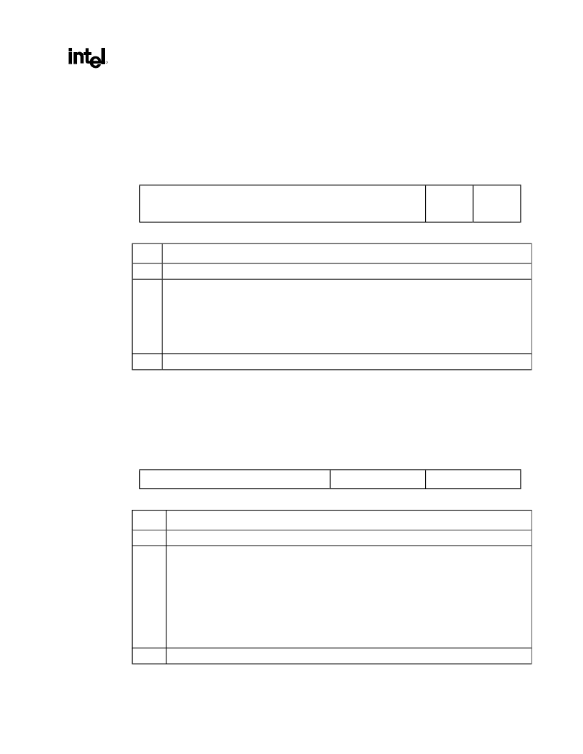
3.8.2.
MSR
I/O (and Memory Offset) Address: 3C2h
Write;
Default:
Access:
Size:
7
Miscellaneous Output
3CCh
Read
00h
See Address above
8 bits
2
1
0
Reserved
A0000h
BFFFFh
Acc En
Reserved
Bit
Descriptions
7:2
Reserved
1
A0000
BFFFFh Access Enable.
VGA Compatibility bit enables access to the display cache at
A0000h
BFFFFh. When disabled, accesses to system memory are blocked in this region (by not
asserting DEVSEL#). This bit does not block processor access to the video linear frame buffer at other
addresses.
0 = Prevent processor access to the display cache (default).
1 = Allow processor access to display cache.
0
Reserved
3.8.3.
GR06
I/O (and Memory Offset) Address:
Default:
Access:
Size:
7
Miscellaneous Register
3CFh (Index=06h)
0Uh (U=Undefined)
Read/Write
8 bits
4
3
2
1
0
Reserved
Memory Map Mode
Reserved
Bit
Description
7:4
Reserved
3:2
Memory Map Mode.
These 2 bits control the mapping of the VGA frame buffer into the processor
address space as follows:
00 = A0000h
BFFFFh
01 = A0000h
AFFFFh
10 = B0000h
B7FFFh
11 = B8000h
BFFFFh
Note: This function is both in standard VGA modes and in extended modes that do not provide linear
frame buffer accesses.
1:0
Reserved
相關PDF資料 |
PDF描述 |
|---|---|
| FWA-25A10F | Fuse |
| FWA-30A10F | Fuse |
| FWA-35A21F | Fuse |
| FWA-40A21F | Fuse |
| FWA-45A21F | Fuse |
相關代理商/技術參數 |
參數描述 |
|---|---|
| FW82815 S L5NQ | 制造商:Intel 功能描述:Graphics and Memory Controller Hub 544-Pin BGA |
| FW82815EM S L4MP | 制造商:Intel 功能描述:GRAPHICS AND MEMORY CONTROLLER HUB (GMCH2-M) |
| FW82815SL5NQ | 制造商:Intel 功能描述: |
| FW828201CA | 制造商:未知廠家 制造商全稱:未知廠家 功能描述:Controller Miscellaneous - Datasheet Reference |
| FW82840 S L3TA | 制造商:Intel 功能描述:Memory Controller Hub 544-Pin BGA |
發(fā)布緊急采購,3分鐘左右您將得到回復。