- 您現(xiàn)在的位置:買賣IC網(wǎng) > PDF目錄369902 > MC68HC11A8 (Motorola, Inc.) 8-Bit Microcontroller(8位微控制器) PDF資料下載
參數(shù)資料
| 型號(hào): | MC68HC11A8 |
| 廠商: | Motorola, Inc. |
| 元件分類: | 8位微控制器 |
| 英文描述: | 8-Bit Microcontroller(8位微控制器) |
| 中文描述: | 8位微控制器(8位微控制器) |
| 文件頁(yè)數(shù): | 47/512頁(yè) |
| 文件大小: | 4071K |
| 代理商: | MC68HC11A8 |
第1頁(yè)第2頁(yè)第3頁(yè)第4頁(yè)第5頁(yè)第6頁(yè)第7頁(yè)第8頁(yè)第9頁(yè)第10頁(yè)第11頁(yè)第12頁(yè)第13頁(yè)第14頁(yè)第15頁(yè)第16頁(yè)第17頁(yè)第18頁(yè)第19頁(yè)第20頁(yè)第21頁(yè)第22頁(yè)第23頁(yè)第24頁(yè)第25頁(yè)第26頁(yè)第27頁(yè)第28頁(yè)第29頁(yè)第30頁(yè)第31頁(yè)第32頁(yè)第33頁(yè)第34頁(yè)第35頁(yè)第36頁(yè)第37頁(yè)第38頁(yè)第39頁(yè)第40頁(yè)第41頁(yè)第42頁(yè)第43頁(yè)第44頁(yè)第45頁(yè)第46頁(yè)當(dāng)前第47頁(yè)第48頁(yè)第49頁(yè)第50頁(yè)第51頁(yè)第52頁(yè)第53頁(yè)第54頁(yè)第55頁(yè)第56頁(yè)第57頁(yè)第58頁(yè)第59頁(yè)第60頁(yè)第61頁(yè)第62頁(yè)第63頁(yè)第64頁(yè)第65頁(yè)第66頁(yè)第67頁(yè)第68頁(yè)第69頁(yè)第70頁(yè)第71頁(yè)第72頁(yè)第73頁(yè)第74頁(yè)第75頁(yè)第76頁(yè)第77頁(yè)第78頁(yè)第79頁(yè)第80頁(yè)第81頁(yè)第82頁(yè)第83頁(yè)第84頁(yè)第85頁(yè)第86頁(yè)第87頁(yè)第88頁(yè)第89頁(yè)第90頁(yè)第91頁(yè)第92頁(yè)第93頁(yè)第94頁(yè)第95頁(yè)第96頁(yè)第97頁(yè)第98頁(yè)第99頁(yè)第100頁(yè)第101頁(yè)第102頁(yè)第103頁(yè)第104頁(yè)第105頁(yè)第106頁(yè)第107頁(yè)第108頁(yè)第109頁(yè)第110頁(yè)第111頁(yè)第112頁(yè)第113頁(yè)第114頁(yè)第115頁(yè)第116頁(yè)第117頁(yè)第118頁(yè)第119頁(yè)第120頁(yè)第121頁(yè)第122頁(yè)第123頁(yè)第124頁(yè)第125頁(yè)第126頁(yè)第127頁(yè)第128頁(yè)第129頁(yè)第130頁(yè)第131頁(yè)第132頁(yè)第133頁(yè)第134頁(yè)第135頁(yè)第136頁(yè)第137頁(yè)第138頁(yè)第139頁(yè)第140頁(yè)第141頁(yè)第142頁(yè)第143頁(yè)第144頁(yè)第145頁(yè)第146頁(yè)第147頁(yè)第148頁(yè)第149頁(yè)第150頁(yè)第151頁(yè)第152頁(yè)第153頁(yè)第154頁(yè)第155頁(yè)第156頁(yè)第157頁(yè)第158頁(yè)第159頁(yè)第160頁(yè)第161頁(yè)第162頁(yè)第163頁(yè)第164頁(yè)第165頁(yè)第166頁(yè)第167頁(yè)第168頁(yè)第169頁(yè)第170頁(yè)第171頁(yè)第172頁(yè)第173頁(yè)第174頁(yè)第175頁(yè)第176頁(yè)第177頁(yè)第178頁(yè)第179頁(yè)第180頁(yè)第181頁(yè)第182頁(yè)第183頁(yè)第184頁(yè)第185頁(yè)第186頁(yè)第187頁(yè)第188頁(yè)第189頁(yè)第190頁(yè)第191頁(yè)第192頁(yè)第193頁(yè)第194頁(yè)第195頁(yè)第196頁(yè)第197頁(yè)第198頁(yè)第199頁(yè)第200頁(yè)第201頁(yè)第202頁(yè)第203頁(yè)第204頁(yè)第205頁(yè)第206頁(yè)第207頁(yè)第208頁(yè)第209頁(yè)第210頁(yè)第211頁(yè)第212頁(yè)第213頁(yè)第214頁(yè)第215頁(yè)第216頁(yè)第217頁(yè)第218頁(yè)第219頁(yè)第220頁(yè)第221頁(yè)第222頁(yè)第223頁(yè)第224頁(yè)第225頁(yè)第226頁(yè)第227頁(yè)第228頁(yè)第229頁(yè)第230頁(yè)第231頁(yè)第232頁(yè)第233頁(yè)第234頁(yè)第235頁(yè)第236頁(yè)第237頁(yè)第238頁(yè)第239頁(yè)第240頁(yè)第241頁(yè)第242頁(yè)第243頁(yè)第244頁(yè)第245頁(yè)第246頁(yè)第247頁(yè)第248頁(yè)第249頁(yè)第250頁(yè)第251頁(yè)第252頁(yè)第253頁(yè)第254頁(yè)第255頁(yè)第256頁(yè)第257頁(yè)第258頁(yè)第259頁(yè)第260頁(yè)第261頁(yè)第262頁(yè)第263頁(yè)第264頁(yè)第265頁(yè)第266頁(yè)第267頁(yè)第268頁(yè)第269頁(yè)第270頁(yè)第271頁(yè)第272頁(yè)第273頁(yè)第274頁(yè)第275頁(yè)第276頁(yè)第277頁(yè)第278頁(yè)第279頁(yè)第280頁(yè)第281頁(yè)第282頁(yè)第283頁(yè)第284頁(yè)第285頁(yè)第286頁(yè)第287頁(yè)第288頁(yè)第289頁(yè)第290頁(yè)第291頁(yè)第292頁(yè)第293頁(yè)第294頁(yè)第295頁(yè)第296頁(yè)第297頁(yè)第298頁(yè)第299頁(yè)第300頁(yè)第301頁(yè)第302頁(yè)第303頁(yè)第304頁(yè)第305頁(yè)第306頁(yè)第307頁(yè)第308頁(yè)第309頁(yè)第310頁(yè)第311頁(yè)第312頁(yè)第313頁(yè)第314頁(yè)第315頁(yè)第316頁(yè)第317頁(yè)第318頁(yè)第319頁(yè)第320頁(yè)第321頁(yè)第322頁(yè)第323頁(yè)第324頁(yè)第325頁(yè)第326頁(yè)第327頁(yè)第328頁(yè)第329頁(yè)第330頁(yè)第331頁(yè)第332頁(yè)第333頁(yè)第334頁(yè)第335頁(yè)第336頁(yè)第337頁(yè)第338頁(yè)第339頁(yè)第340頁(yè)第341頁(yè)第342頁(yè)第343頁(yè)第344頁(yè)第345頁(yè)第346頁(yè)第347頁(yè)第348頁(yè)第349頁(yè)第350頁(yè)第351頁(yè)第352頁(yè)第353頁(yè)第354頁(yè)第355頁(yè)第356頁(yè)第357頁(yè)第358頁(yè)第359頁(yè)第360頁(yè)第361頁(yè)第362頁(yè)第363頁(yè)第364頁(yè)第365頁(yè)第366頁(yè)第367頁(yè)第368頁(yè)第369頁(yè)第370頁(yè)第371頁(yè)第372頁(yè)第373頁(yè)第374頁(yè)第375頁(yè)第376頁(yè)第377頁(yè)第378頁(yè)第379頁(yè)第380頁(yè)第381頁(yè)第382頁(yè)第383頁(yè)第384頁(yè)第385頁(yè)第386頁(yè)第387頁(yè)第388頁(yè)第389頁(yè)第390頁(yè)第391頁(yè)第392頁(yè)第393頁(yè)第394頁(yè)第395頁(yè)第396頁(yè)第397頁(yè)第398頁(yè)第399頁(yè)第400頁(yè)第401頁(yè)第402頁(yè)第403頁(yè)第404頁(yè)第405頁(yè)第406頁(yè)第407頁(yè)第408頁(yè)第409頁(yè)第410頁(yè)第411頁(yè)第412頁(yè)第413頁(yè)第414頁(yè)第415頁(yè)第416頁(yè)第417頁(yè)第418頁(yè)第419頁(yè)第420頁(yè)第421頁(yè)第422頁(yè)第423頁(yè)第424頁(yè)第425頁(yè)第426頁(yè)第427頁(yè)第428頁(yè)第429頁(yè)第430頁(yè)第431頁(yè)第432頁(yè)第433頁(yè)第434頁(yè)第435頁(yè)第436頁(yè)第437頁(yè)第438頁(yè)第439頁(yè)第440頁(yè)第441頁(yè)第442頁(yè)第443頁(yè)第444頁(yè)第445頁(yè)第446頁(yè)第447頁(yè)第448頁(yè)第449頁(yè)第450頁(yè)第451頁(yè)第452頁(yè)第453頁(yè)第454頁(yè)第455頁(yè)第456頁(yè)第457頁(yè)第458頁(yè)第459頁(yè)第460頁(yè)第461頁(yè)第462頁(yè)第463頁(yè)第464頁(yè)第465頁(yè)第466頁(yè)第467頁(yè)第468頁(yè)第469頁(yè)第470頁(yè)第471頁(yè)第472頁(yè)第473頁(yè)第474頁(yè)第475頁(yè)第476頁(yè)第477頁(yè)第478頁(yè)第479頁(yè)第480頁(yè)第481頁(yè)第482頁(yè)第483頁(yè)第484頁(yè)第485頁(yè)第486頁(yè)第487頁(yè)第488頁(yè)第489頁(yè)第490頁(yè)第491頁(yè)第492頁(yè)第493頁(yè)第494頁(yè)第495頁(yè)第496頁(yè)第497頁(yè)第498頁(yè)第499頁(yè)第500頁(yè)第501頁(yè)第502頁(yè)第503頁(yè)第504頁(yè)第505頁(yè)第506頁(yè)第507頁(yè)第508頁(yè)第509頁(yè)第510頁(yè)第511頁(yè)第512頁(yè)
M68HC11
REFERENCE MANUAL
PINS AND CONNECTIONS
MOTOROLA
2-25
interfere with normal operation of an MCU signal. For example, a low-pass filter on an
address or data line of an expanded MCU system would introduce significant delays
to these signals, dramatically limiting the maximum operating speed of the system.
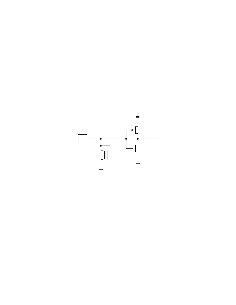
2.4.3 Internal Circuitry — Digital Input-Only Pin
Figure 2-15
shows the MOS circuitry for a digital input-only pin. The gates of input
buffer [3] are very high impedance for all voltages that would ever be applied to the
pin. The thick-field protection device [2] normally prevents the pin voltage from reach-
ing levels that could damage the gates of the input buffer. The exact circuitry of the
input buffer may be different for different digital inputs (e.g., to provide hysteresis,
etc.), but only device gates will be connected directly to the pin. Allowing a pin to float
(or be driven) to a midsupply level can result in both the N- and P-channel devices in
the input buffer simultaneously being partially on, which causes excess current and
noise on the V
DD
/V
SS
power supply. Port E inputs are exceptions because they are
specifically designed to be driven by analog levels.
Figure 2-15 Internal Circuitry — Digital Input-Only Pin
If a digital input pin (see
Figure 2-15
) is driven with voltages below V
SS
, the thick-field
protection device [2] forms an inherent diode junction to V
SS
, which conducts when the
pin voltage gets more than a diode drop below V
SS
. As the pin voltage is driven more
negative with respect to V
SS
, current increases. These currents have a tendency to
influence the die substrate in the area around the protection device, thus affecting the
electrical characteristics of devices in the vicinity. When the pin current is increased to
very high levels (typically more than 100 mA, specified limit is 25 mA), physical dam-
age can result.
As voltage at [1] is driven above V
DD
, the protection device will begin to conduct and
tend to clamp the input voltage to protect input buffer [3]. The voltage at which this con-
dition will occur varies significantly from lot to lot and over the operating temperature
range. At room temperature, the pin typically does not draw any current until approxi-
mately 20 V; at 125
°
, the pin may start conducting at a slightly lower level. Up to this
point, the pin appears to function normally and will return a logic one if read. As the pin
P
N
VDD
T
P
PIN
N
[1]
[2]
[3]
INPUT
BUFFER
相關(guān)PDF資料 |
PDF描述 |
|---|---|
| MC68HC11E32 | 8-Bit Microcontroller(8位微控制器) |
| MC68HC11K1 | 8-Bit Microcontroller(8位微控制器) |
| MC68HC12 | The MC68HC912DT128A microcontroller unit (MCU) is a 16-bit device composed of standard on-chip peripherals including a 16-bit central processing unit |
| MC68HC16Z3 | 16-BIT MODULAR MICROCONTROLLER |
| MC68HC16Z3PD | 16-BIT MODULAR MICROCONTROLLER |
相關(guān)代理商/技術(shù)參數(shù) |
參數(shù)描述 |
|---|---|
| MC68HC11A8BCFN2 | 制造商:MOTOROLA 制造商全稱:Motorola, Inc 功能描述:HCMOS Single-Chip Microcontroller |
| MC68HC11A8BCFU2 | 制造商:MOTOROLA 制造商全稱:Motorola, Inc 功能描述:HCMOS Single-Chip Microcontroller |
| MC68HC11A8BCP2 | 制造商:MOTOROLA 制造商全稱:Motorola, Inc 功能描述:HCMOS Single-Chip Microcontroller |
| MC68HC11A8BMP2 | 制造商:MOTOROLA 制造商全稱:Motorola, Inc 功能描述:HCMOS Single-Chip Microcontroller |
| MC68HC11A8BVP2 | 制造商:MOTOROLA 制造商全稱:Motorola, Inc 功能描述:HCMOS Single-Chip Microcontroller |
發(fā)布緊急采購(gòu),3分鐘左右您將得到回復(fù)。