- 您現(xiàn)在的位置:買賣IC網(wǎng) > PDF目錄67681 > IBM21P100BGC PCI BUS CONTROLLER, PBGA304 PDF資料下載
參數(shù)資料
| 型號: | IBM21P100BGC |
| 元件分類: | 總線控制器 |
| 英文描述: | PCI BUS CONTROLLER, PBGA304 |
| 封裝: | 31 X 31 MM, PLASTIC, BGA-304 |
| 文件頁數(shù): | 31/144頁 |
| 文件大小: | 5197K |
| 代理商: | IBM21P100BGC |
第1頁第2頁第3頁第4頁第5頁第6頁第7頁第8頁第9頁第10頁第11頁第12頁第13頁第14頁第15頁第16頁第17頁第18頁第19頁第20頁第21頁第22頁第23頁第24頁第25頁第26頁第27頁第28頁第29頁第30頁當前第31頁第32頁第33頁第34頁第35頁第36頁第37頁第38頁第39頁第40頁第41頁第42頁第43頁第44頁第45頁第46頁第47頁第48頁第49頁第50頁第51頁第52頁第53頁第54頁第55頁第56頁第57頁第58頁第59頁第60頁第61頁第62頁第63頁第64頁第65頁第66頁第67頁第68頁第69頁第70頁第71頁第72頁第73頁第74頁第75頁第76頁第77頁第78頁第79頁第80頁第81頁第82頁第83頁第84頁第85頁第86頁第87頁第88頁第89頁第90頁第91頁第92頁第93頁第94頁第95頁第96頁第97頁第98頁第99頁第100頁第101頁第102頁第103頁第104頁第105頁第106頁第107頁第108頁第109頁第110頁第111頁第112頁第113頁第114頁第115頁第116頁第117頁第118頁第119頁第120頁第121頁第122頁第123頁第124頁第125頁第126頁第127頁第128頁第129頁第130頁第131頁第132頁第133頁第134頁第135頁第136頁第137頁第138頁第139頁第140頁第141頁第142頁第143頁第144頁
IBM21P100BGC
IBM 133 PCI-X Bridge R2.0
JTAG Boundary Scan
Page 126 of 144
ppb20_jtag.fm.01
October 15, 2001
9.3 Bypass Register
This register is a 1-bit shift register that provides a single bit scan path between the JTG_TDI input and the
JTG_TDO output. This abbreviated scan path is selected by the BYPASS instruction code and is used to
shorten the overall scan ring length during board-level testing when the bridge is not involved.
9.4 Device ID Register
This register, defined by IEEE Standard 1149.1, identifies IBM as the manufacturer of the IBM 133 PCI-X
Bridge R2.0 and provides a portion of the die part number and a revision code for the device.
9.5 Boundary-Scan Register
The Boundary-Scan register is formed by connecting boundary scan cells placed at the device’s signal pins
into a shift register path. The input to the shift register is the JTG_TDI signal and the output from the shift
register is the JTG_TDO signal. When selected and controlled properly by the TAP Controller, this structure
provides the output drive and input visibility features necessary for effective boundary-scan testing.
Several varieties of boundary-scan cells are possible, selected according to the function of the signal pin with
which they are associated:
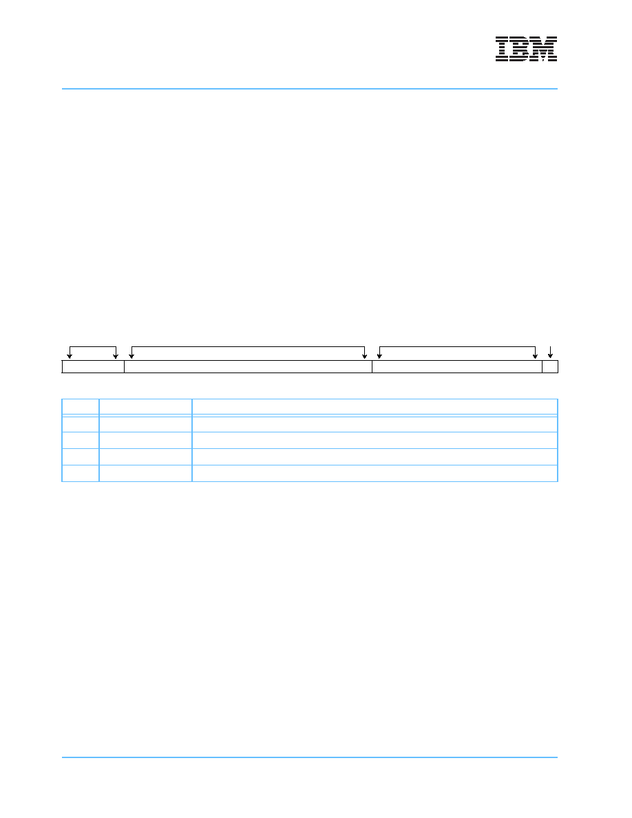
Width
32 bits
Access
Read only
Reset Value
x‘1490049’
Version
Part Number
Manufacturer ID
Fi
x
e
d
31 30 29 28 27 26 25 24 23 22 21 20 19 18 17 16 15 14 13 12 11 10
9
8
7
6
5
4
3
2
1
0
Bits
Access
Field Name and Description
31:28
RO
Version number of the device.
27:12
RO
Last four hex digits of the BEOL die part number.
11:1
RO
JEDEC-assigned identifier for manufacturer (IBM).
0
RO
Fixed bit equal to b‘1’.
Input-only pins:
For device inputs that are not shared with component test functions, the boundary-
scan cell IBM1149_BSR_BIDIIN is used. Inputs that are shared with component
test functions use the IBM1149_BSR_IN boundary-scan cell. Both have the BSDL
function label of ‘INPUT’.
相關(guān)PDF資料 |
PDF描述 |
|---|---|
| IBM25403GCX-3JC76C2 | RISC PROCESSOR, PQFP16 |
| IBM25405GP-3BA200C2 | RISC PROCESSOR, PBGA456 |
| IBM25EMPPC603EFG-100 | 32-BIT, 100 MHz, RISC PROCESSOR, PQFP240 |
| IBM25EMPPC603EBG-100 | 32-BIT, 100 MHz, RISC PROCESSOR, CBGA255 |
| IBM25EMPPC740LDBC4000 | 32-BIT, 400 MHz, RISC PROCESSOR, CBGA255 |
相關(guān)代理商/技術(shù)參數(shù) |
參數(shù)描述 |
|---|---|
| IBM24L5086 | 制造商:AVED MEMORY PRODUCTS 功能描述: 制造商:AVED Memory Products 功能描述: |
| IBM25403GCX-3BC80C2 | 制造商:IBM 功能描述:RISC PROCESSOR, 160 Pin Plastic BGA |
| IBM25403GCX-3JC50C2 | 制造商:IBM 功能描述:403GCX-3JC50C2 |
| IBM25403GCX-3JC66C2 | 制造商:IBM 功能描述: |
| IBM25403GCX3JC76C2 | 制造商:IBM 功能描述: |
發(fā)布緊急采購,3分鐘左右您將得到回復(fù)。