- 您現(xiàn)在的位置:買賣IC網(wǎng) > PDF目錄379500 > UPD488448FB-C80-45-DQ1 (NEC Corp.) 128 M-bit Direct Rambus⑩ DRAM PDF資料下載
參數(shù)資料
| 型號: | UPD488448FB-C80-45-DQ1 |
| 廠商: | NEC Corp. |
| 英文描述: | 128 M-bit Direct Rambus⑩ DRAM |
| 中文描述: | 128 M位DRAM的直接Rambus的⑩ |
| 文件頁數(shù): | 46/80頁 |
| 文件大?。?/td> | 1902K |
| 代理商: | UPD488448FB-C80-45-DQ1 |
第1頁第2頁第3頁第4頁第5頁第6頁第7頁第8頁第9頁第10頁第11頁第12頁第13頁第14頁第15頁第16頁第17頁第18頁第19頁第20頁第21頁第22頁第23頁第24頁第25頁第26頁第27頁第28頁第29頁第30頁第31頁第32頁第33頁第34頁第35頁第36頁第37頁第38頁第39頁第40頁第41頁第42頁第43頁第44頁第45頁當(dāng)前第46頁第47頁第48頁第49頁第50頁第51頁第52頁第53頁第54頁第55頁第56頁第57頁第58頁第59頁第60頁第61頁第62頁第63頁第64頁第65頁第66頁第67頁第68頁第69頁第70頁第71頁第72頁第73頁第74頁第75頁第76頁第77頁第78頁第79頁第80頁
Data Sheet M14837EJ3V0DS00
46
μ
PD488448 for Rev. P
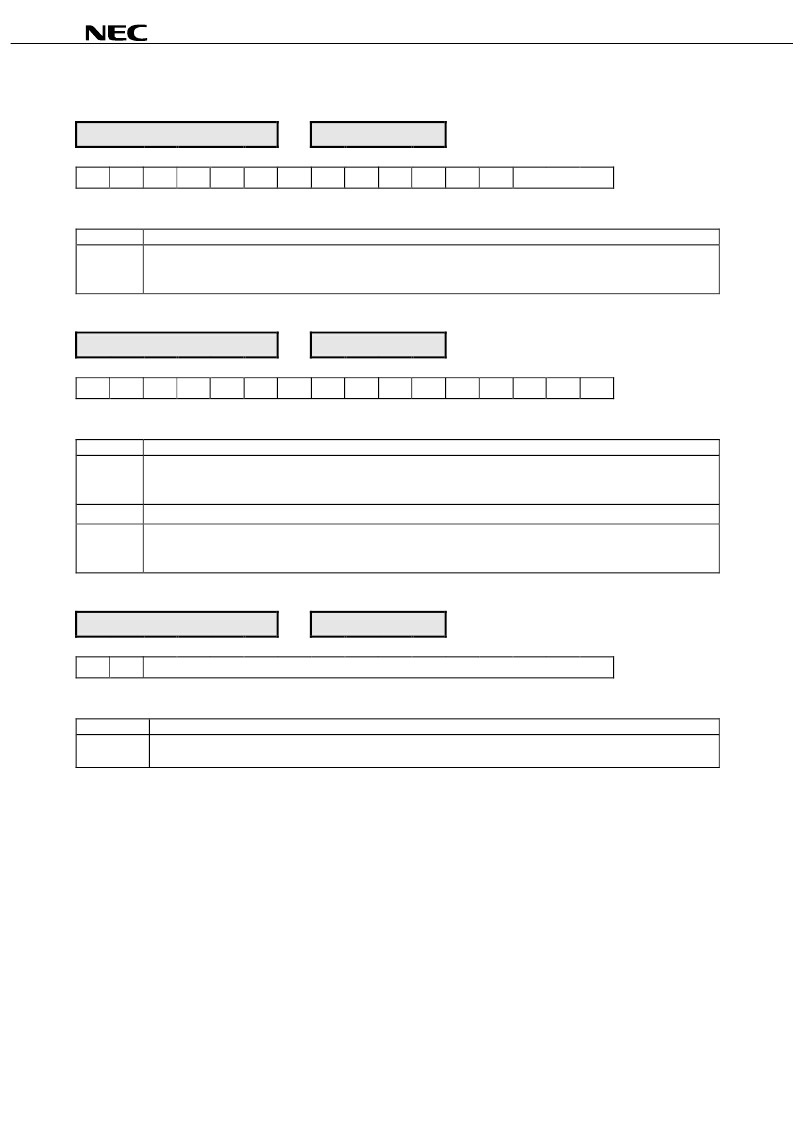
Figure 22-1 Control Registers (6/7)
Control Register : TCDLY1
Address : 04a
16
15
14
13
12
11
10
9
8
7
6
5
4
3
2
1
0
0
0
0
0
0
0
0
0
0
0
0
0
0
TCDLY1
Read/write register.
Reset value is undefined.
Field
Description
Specifies the value of the t
CDLY1-C
core parameter in t
CYCLE
units. This adds a programmable delay to Q (read data)
packets, permitting round trip read to delay all devices to be equalized. This field may be written with the values “000”
(0
t
CYCLE
) through “010” (2
t
CYCLE
). Refer to TPARM Register for more details.
TCDLY1
Control Register : SKIP
Address : 04b
16
15
14
13
12
11
10
9
8
7
6
5
4
3
2
1
0
0
0
0
AS
MSE
MS
0
0
0
0
0
0
0
0
0
0
Read/write register (except AS field).
Reset value is zero.
Field
Description
Manual skip (MS must be 1 when MSE=1). > During initialization, the RDRAMs at the furthest point in the fifth read
domain may have selected the AS=0 value, placing them at the closest point in a sixth read domain. Setting the
MSE/MS fields to 1/1 overrides the autoskip value and returns hem to 111 he furthest point of the fifth read domain.
Manual skip enable (0=auto, 1=manual ).
MS
MSE
AS
Autoskip. Read-only value determined by autoskip circuit and stored when SETF serial command is received by
RDRAM during initialization. In Figure34-1, AS=1 corresponds to the early Q(a1) packet and AS=0 to the Q(a1) packet
one t
CYCLE
later for the four uncertain cases.
Control Register : TCYCLE
Address : 04c
16
15
14
13
12
11
10
9
8
7
6
5
4
3
2
1
0
0
0
TCYCLE13..0
Read/write register.
Reset value is undefined.
Field
Description
Specifies the value of the t
CYCLE
datasheet parameter in 64ps units. For the t
CYCLE,MIN
of 2.50 ns (2500ps), this field
should be written with the “00027
16
” (39
64ps).
TCYCLE13..0
相關(guān)PDF資料 |
PDF描述 |
|---|---|
| UPD488448FB-C80-45-DQ2 | 128 M-bit Direct Rambus⑩ DRAM |
| UPD488448FB-C71-45-DQ1 | 128 M-bit Direct Rambus⑩ DRAM |
| UPD488448FB-C71-45-DQ2 | 128 M-bit Direct Rambus⑩ DRAM |
| UPD488448FB-C60-53-DQ2 | 128 M-bit Direct Rambus⑩ DRAM |
| UPD488448FF-C80-45-DQ1 | 128 M-bit Direct Rambus⑩ DRAM |
相關(guān)代理商/技術(shù)參數(shù) |
參數(shù)描述 |
|---|---|
| UPD4990AG-A | 制造商:Renesas Electronics 功能描述:Cut Tape |
| UPD4991ACX-A | 制造商:Renesas Electronics Corporation 功能描述: |
| UPD4992CX-A | 制造商:Renesas Electronics 功能描述:Cut Tape |
| UPD50256CP15 | 制造商:HIT 功能描述:50256 HITACHI'86 SMT N9F8A |
| UPD50256CP-15 | 制造商:HIT 功能描述:50256 HITACHI'86 SMT N9F8A |
發(fā)布緊急采購,3分鐘左右您將得到回復(fù)。