- 您現(xiàn)在的位置:買賣IC網(wǎng) > PDF目錄379500 > UPD488448FB-C80-45-DQ1 (NEC Corp.) 128 M-bit Direct Rambus⑩ DRAM PDF資料下載
參數(shù)資料
| 型號: | UPD488448FB-C80-45-DQ1 |
| 廠商: | NEC Corp. |
| 英文描述: | 128 M-bit Direct Rambus⑩ DRAM |
| 中文描述: | 128 M位DRAM的直接Rambus的⑩ |
| 文件頁數(shù): | 45/80頁 |
| 文件大小: | 1902K |
| 代理商: | UPD488448FB-C80-45-DQ1 |
第1頁第2頁第3頁第4頁第5頁第6頁第7頁第8頁第9頁第10頁第11頁第12頁第13頁第14頁第15頁第16頁第17頁第18頁第19頁第20頁第21頁第22頁第23頁第24頁第25頁第26頁第27頁第28頁第29頁第30頁第31頁第32頁第33頁第34頁第35頁第36頁第37頁第38頁第39頁第40頁第41頁第42頁第43頁第44頁當前第45頁第46頁第47頁第48頁第49頁第50頁第51頁第52頁第53頁第54頁第55頁第56頁第57頁第58頁第59頁第60頁第61頁第62頁第63頁第64頁第65頁第66頁第67頁第68頁第69頁第70頁第71頁第72頁第73頁第74頁第75頁第76頁第77頁第78頁第79頁第80頁
Data Sheet M14837EJ3V0DS00
45
μ
PD488448 for Rev. P
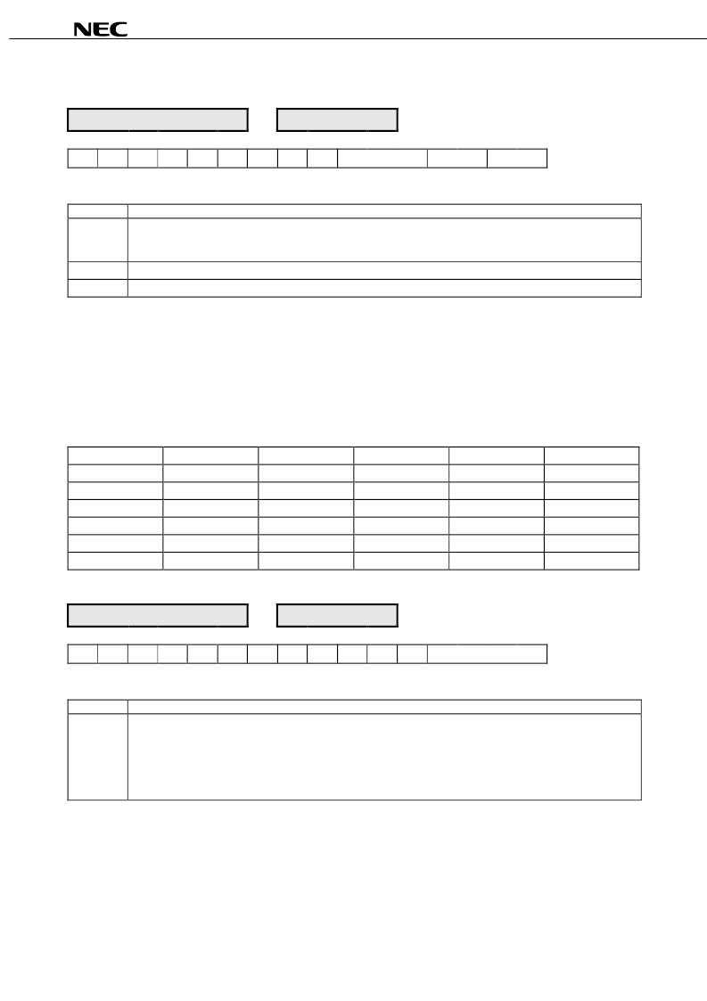
Figure 22-1 Control Registers (5/7)
Control Register : TPARM
Address : 048
16
15
14
13
12
11
10
9
8
7
6
5
4
3
2
1
0
0
0
0
0
0
0
0
0
0
TCDLY0
TCLS
TCAL
Read/write register.
Reset value is undefined.
Field
Description
Specifies the t
CDLY0-C
core parameter in t
CYCLE
units. This adds a programmable delay to Q (read data) packets,
permitting round trip read delay to all device to be equalized. This field may be written with the values “010” (2
t
CYCLE
)
through “101” (5
t
CYCLE
).
Specifies the t
CLS-C
core parameter in t
CYCLE
units. Should be “10” (2
t
CYCLE
).
TCDLY0
TCLS1..0
TCAS1..0
The equations relating the core parameters to the datasheet parameters follow:
t
CAS-C
=2
t
CYCLE
t
CLS-C
=2
t
CYCLE
t
CPS-C
=1
t
CYCLE
Not programmable
Specifies the t
CAS-C
core parameter in t
CYCLE
units. This should be “10” (2
t
CYCLE
).
t
OFFP
=t
CPS-C
+ t
CAS-C
+ t
CLS-C
- 1
t
CYCLE
=4
t
CYCLE
t
RCD
=t
RCD-C
+ 1
t
CYCLE
– t
CLS-C
=t
RCD-C
- 1
t
CYCLE
t
CAC
=3
t
CYCLE
+ t
CLS-C
+ t
CDLY0-C
+ t
CDLY1-C
(see table below programming ranges)
TCDLY0
t
CDLY0-C
TCDLY1
t
CDLY1-C
t
CAC
@t
CYCLE
=3.30 ns t
CAC
@t
CYCLE
=2.50 ns
010
2
t
CYCLE
000
0
t
CYCLE
7
t
CYCLE
not allowed
011
3
t
CYCLE
000
0
t
CYCLE
8
t
CYCLE
8
t
CYCLE
011
3
t
CYCLE
001
1
t
CYCLE
9
t
CYCLE
9
t
CYCLE
011
3
t
CYCLE
010
2
t
CYCLE
10
t
CYCLE
10
t
CYCLE
100
4
t
CYCLE
010
2
t
CYCLE
11
t
CYCLE
11
t
CYCLE
101
5
t
CYCLE
010
2
t
CYCLE
12
t
CYCLE
12
t
CYCLE
Control Register : TFRM
Address : 049
16
15
14
13
12
11
10
9
8
7
6
5
4
3
2
1
0
0
0
0
0
0
0
0
0
0
0
0
0
TFRM3..0
Read/write register.
Reset value is undefined.
Field
Description
Specifies the position of the framing point in t
CYCLE
units. This value must be greater than or equal to the t
FRM,MIN
parameter. This is the minimum offset between a ROW packet (which places a device at ATTN) and the first COL
packet (directed to that device) which must be framed. This field may be written with the value “0111” (7
t
CYCLE
)
through “1010” (10
t
CYCLE
). TFRM is usually set to the value which matches the lagest t
RCD,MIN
parameter (modulo
4
t
CYCLE
) that is present in an RDRAM in the memory system. Thus, if an RDRAM with t
RCD,MIN
=11
t
CYCLE
were
present, then TFRM would be programmed to 7
t
CYCLE
.
TFRM3..0
相關(guān)PDF資料 |
PDF描述 |
|---|---|
| UPD488448FB-C80-45-DQ2 | 128 M-bit Direct Rambus⑩ DRAM |
| UPD488448FB-C71-45-DQ1 | 128 M-bit Direct Rambus⑩ DRAM |
| UPD488448FB-C71-45-DQ2 | 128 M-bit Direct Rambus⑩ DRAM |
| UPD488448FB-C60-53-DQ2 | 128 M-bit Direct Rambus⑩ DRAM |
| UPD488448FF-C80-45-DQ1 | 128 M-bit Direct Rambus⑩ DRAM |
相關(guān)代理商/技術(shù)參數(shù) |
參數(shù)描述 |
|---|---|
| UPD4990AG-A | 制造商:Renesas Electronics 功能描述:Cut Tape |
| UPD4991ACX-A | 制造商:Renesas Electronics Corporation 功能描述: |
| UPD4992CX-A | 制造商:Renesas Electronics 功能描述:Cut Tape |
| UPD50256CP15 | 制造商:HIT 功能描述:50256 HITACHI'86 SMT N9F8A |
| UPD50256CP-15 | 制造商:HIT 功能描述:50256 HITACHI'86 SMT N9F8A |
發(fā)布緊急采購,3分鐘左右您將得到回復(fù)。