- 您現(xiàn)在的位置:買賣IC網(wǎng) > PDF目錄379500 > UPD488448FB-C80-45-DQ1 (NEC Corp.) 128 M-bit Direct Rambus⑩ DRAM PDF資料下載
參數(shù)資料
| 型號(hào): | UPD488448FB-C80-45-DQ1 |
| 廠商: | NEC Corp. |
| 英文描述: | 128 M-bit Direct Rambus⑩ DRAM |
| 中文描述: | 128 M位DRAM的直接Rambus的⑩ |
| 文件頁數(shù): | 32/80頁 |
| 文件大小: | 1902K |
| 代理商: | UPD488448FB-C80-45-DQ1 |
第1頁第2頁第3頁第4頁第5頁第6頁第7頁第8頁第9頁第10頁第11頁第12頁第13頁第14頁第15頁第16頁第17頁第18頁第19頁第20頁第21頁第22頁第23頁第24頁第25頁第26頁第27頁第28頁第29頁第30頁第31頁當(dāng)前第32頁第33頁第34頁第35頁第36頁第37頁第38頁第39頁第40頁第41頁第42頁第43頁第44頁第45頁第46頁第47頁第48頁第49頁第50頁第51頁第52頁第53頁第54頁第55頁第56頁第57頁第58頁第59頁第60頁第61頁第62頁第63頁第64頁第65頁第66頁第67頁第68頁第69頁第70頁第71頁第72頁第73頁第74頁第75頁第76頁第77頁第78頁第79頁第80頁
Data Sheet M14837EJ3V0DS00
32
μ
PD488448 for Rev. P
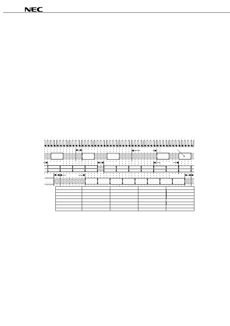
18. Interleaved RRWW - Example
Figure 18-1 shows a steady-state sequence of 2-dualoct RD/RD/WR/WR.. transactions directed to non-adjacent
banks of a single RDRAM. This is similar to the interleaved write and read examples in Figure 16-1 and Figure 17-1
except that bubble cycles need to be inserted by the controller at read/write boundaries. The DQ data pin efficiency
for the example in Figure 18-1 is 32/42 or 76%. If there were more RDRAMs on the Channel, the DQ pin efficiency
would approach 32/34 or 94% for the two-dualoct RRWW sequence (this case is not shown).
In Figure 18-1, the first bubble type t
CBUB1
is inserted by the controller between a RD and WR command on the COL
pins. This bubble accounts for the round-trip propagation delay that is seen by read data, and is explained in detail in
Figure 4-1. This bubble appears on the DQA and DQB pins as t
DBUB1
between a write data dualoct D and read data
dualoct Q. This bubble also appears on the ROW pins as t
RBUB1
.
The second bubble type t
CBUB2
is inserted (as a NOCOP command) by the controller between a WR and RD
command on the COL pins when there is a WR-WR-RD sequence to the same device. This bubble enables write
data to be retired from the write buffer without being lost, and is explained in detail in Figure 15-2. There would be no
bubble if address c0 and address d0 were directed to different devices. This bubble appears on the DQA and DQB
pins as t
DBUB2
between a write data dualoct D and read data dualoct Q. This bubble also appears on the ROW pins
as t
RBUB2
.
Figure 18-1 Interleaved RRWW Sequence with Two Dualoct Data Length
CTM/CFM
DQA7..0
DQB7..0
COL4
..COL0
ROW2
..ROW0
T
0
T
4
T
8
T
12
T
1
T
5
T
9
T
13
T
2
T
6
T
10
T
14
T
3
T
7
T
11
T
15
T
16
T
20
T
24
T
28
T
17
T
21
T
25
T
29
T
18
T
22
T
26
T
30
T
19
T
23
T
27
T
31
T
32
T
36
T
40
T
44
T
33
T
37
T
41
T
45
T
34
T
38
T
42
T
46
T
35
T
39
T
43
T
47
ACT a0
MSK (b2)
WRA c2
MSK (b1)
WR c1
WR b1
MSK (y2)
WRA b2
PREX a3
D (b2)
D (b1)
ACT b0
ACT c0
ACT d0
ACT e0
RD a1
RD a2
PREX z3
Q (a2)
Q (a1)
MSK (c1)
D (c1)
NOCOP
MSK (c2)
RDd0
D (c2)
t
RBUB1
RDf
Q (z2)
Q (z1)
D (y2)
RD z1
RD z2
t
CBUB1
t
DBUB1
t
DBUB1
t
DBUB2
t
CBUB2
t
RBUB2
t
CBUB2
NOCOP
f3 = {Da,Ba+2}
Transaction f: WR
f0 = {Da,Ba+2,Rf}
f1 = {Da,Ba+2,Cf1}
f2= {Da,Ba+2,Cf2}
e3 = {Da,Ba}
Transaction e: RD
e0 = {Da,Ba,Re}
e1 = {Da,Ba,Ce1}
e2= {Da,Ba,Ce2}
d3 = {Da,Ba+6}
Transaction d: RD
d0 = {Da,Ba+6,Rd}
d1 = {Da,Ba+6,Cd1}
d2= {Da,Ba+6,Cd2}
c3 = {Da,Ba+4}
Transaction c: WR
c0 = {Da,Ba+4,Rc}
c1 = {Da,Ba+4,Cc1}
c2= {Da,Ba+4,Cc2}
b3 = {Da,Ba+2}
Transaction b: WR
b0 = {Da,Ba+2,Rb}
b1 = {Da,Ba+2,Cb1}
b2= {Da,Ba+2,Cb2}
a3 = {Da,Ba}
Transaction a: RD
a0 = {Da,Ba,Ra}
a1 = {Da,Ba,Ca1}
a2= {Da,Ba,Ca2}
z3 = {Da,Ba+6}
Transaction z: RD
z0 = {Da,Ba+6,Rz}
z1 = {Da,Ba+6,Cz1}
z2= {Da,Ba+6,Cz2}
y3 = {Da,Ba+4}
Transaction y: WR
y0 = {Da,Ba+4,Ry}
y1 = {Da,Ba+4,Cy1}
y2= {Da,Ba+4,Cy2}
Transaction e can use the
same bank as transaction a
相關(guān)PDF資料 |
PDF描述 |
|---|---|
| UPD488448FB-C80-45-DQ2 | 128 M-bit Direct Rambus⑩ DRAM |
| UPD488448FB-C71-45-DQ1 | 128 M-bit Direct Rambus⑩ DRAM |
| UPD488448FB-C71-45-DQ2 | 128 M-bit Direct Rambus⑩ DRAM |
| UPD488448FB-C60-53-DQ2 | 128 M-bit Direct Rambus⑩ DRAM |
| UPD488448FF-C80-45-DQ1 | 128 M-bit Direct Rambus⑩ DRAM |
相關(guān)代理商/技術(shù)參數(shù) |
參數(shù)描述 |
|---|---|
| UPD4990AG-A | 制造商:Renesas Electronics 功能描述:Cut Tape |
| UPD4991ACX-A | 制造商:Renesas Electronics Corporation 功能描述: |
| UPD4992CX-A | 制造商:Renesas Electronics 功能描述:Cut Tape |
| UPD50256CP15 | 制造商:HIT 功能描述:50256 HITACHI'86 SMT N9F8A |
| UPD50256CP-15 | 制造商:HIT 功能描述:50256 HITACHI'86 SMT N9F8A |
發(fā)布緊急采購,3分鐘左右您將得到回復(fù)。