- 您現(xiàn)在的位置:買賣IC網(wǎng) > PDF目錄379500 > UPD488448FB-C80-45-DQ1 (NEC Corp.) 128 M-bit Direct Rambus⑩ DRAM PDF資料下載
參數(shù)資料
| 型號(hào): | UPD488448FB-C80-45-DQ1 |
| 廠商: | NEC Corp. |
| 英文描述: | 128 M-bit Direct Rambus⑩ DRAM |
| 中文描述: | 128 M位DRAM的直接Rambus的⑩ |
| 文件頁(yè)數(shù): | 15/80頁(yè) |
| 文件大小: | 1902K |
| 代理商: | UPD488448FB-C80-45-DQ1 |
第1頁(yè)第2頁(yè)第3頁(yè)第4頁(yè)第5頁(yè)第6頁(yè)第7頁(yè)第8頁(yè)第9頁(yè)第10頁(yè)第11頁(yè)第12頁(yè)第13頁(yè)第14頁(yè)當(dāng)前第15頁(yè)第16頁(yè)第17頁(yè)第18頁(yè)第19頁(yè)第20頁(yè)第21頁(yè)第22頁(yè)第23頁(yè)第24頁(yè)第25頁(yè)第26頁(yè)第27頁(yè)第28頁(yè)第29頁(yè)第30頁(yè)第31頁(yè)第32頁(yè)第33頁(yè)第34頁(yè)第35頁(yè)第36頁(yè)第37頁(yè)第38頁(yè)第39頁(yè)第40頁(yè)第41頁(yè)第42頁(yè)第43頁(yè)第44頁(yè)第45頁(yè)第46頁(yè)第47頁(yè)第48頁(yè)第49頁(yè)第50頁(yè)第51頁(yè)第52頁(yè)第53頁(yè)第54頁(yè)第55頁(yè)第56頁(yè)第57頁(yè)第58頁(yè)第59頁(yè)第60頁(yè)第61頁(yè)第62頁(yè)第63頁(yè)第64頁(yè)第65頁(yè)第66頁(yè)第67頁(yè)第68頁(yè)第69頁(yè)第70頁(yè)第71頁(yè)第72頁(yè)第73頁(yè)第74頁(yè)第75頁(yè)第76頁(yè)第77頁(yè)第78頁(yè)第79頁(yè)第80頁(yè)
Data Sheet M14837EJ3V0DS00
15
μ
PD488448 for Rev. P
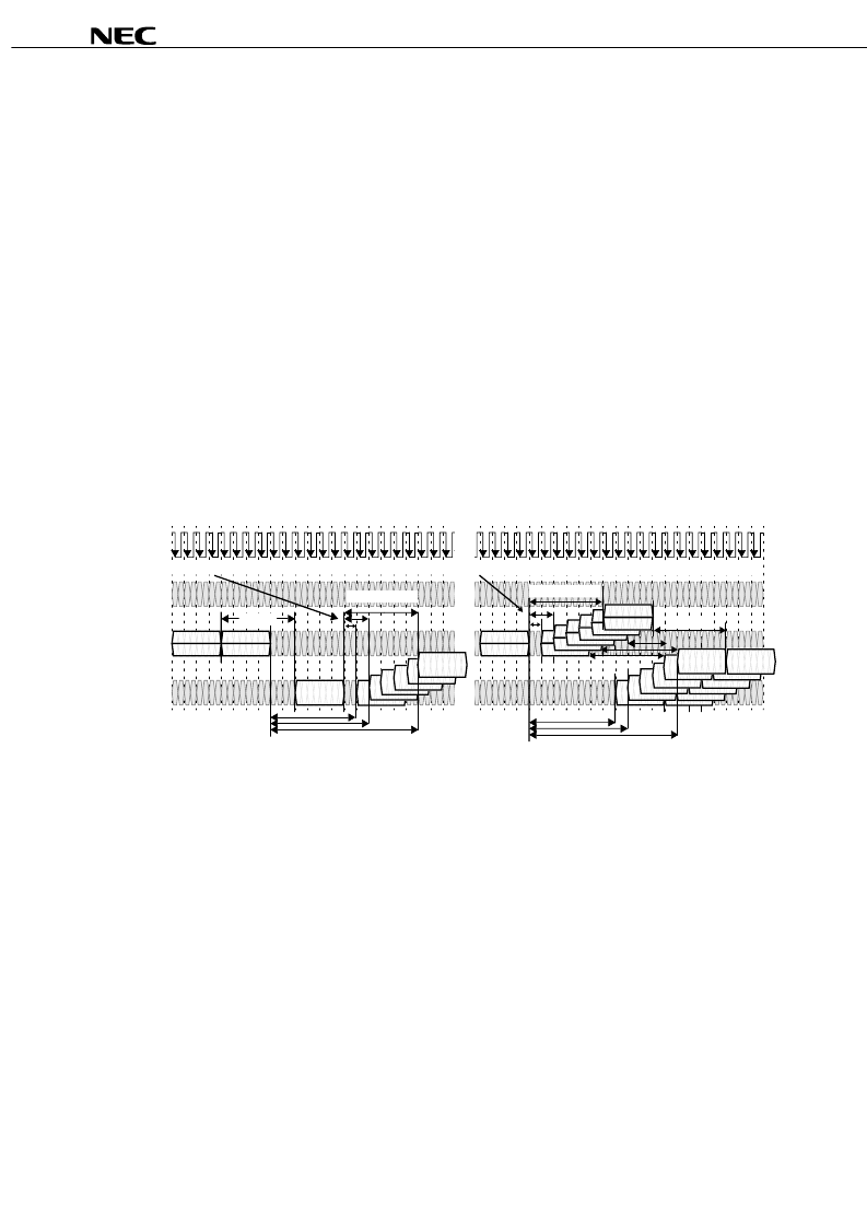
4. DQ Packet Timing
Figure 4-1 shows the timing relationship of COLC packets with D and Q data packets. This document uses a
specific convention for measuring time intervals between packets: all packets on the ROW and COL pins (ROWA,
ROWR, COLC, COLM, COLX) use the trailing edge of the packet as a reference point, and all packets on the
DQA/DQB pins (D and Q) use the leading edge of the packet as a reference point.
An RD or RDA command will transmit a dualoct of read data Q a time t
CAC
later. This time includes one to five
cycles of round-trip propagation delay on the Channel. The t
CAC
parameter may be programmed to a one of a range
of values (7, 8, 9, 10, 11, or 12 t
CYCLE
). The value chosen depends upon the number of RDRAM devices on the
Channel and the RDRAM timing bin. See Figure 22-1(5/7) “
TPARM Register
” for more information.
A WR or WRA command will receive a dualoct of write data D a time t
CWD
later. This time does not need to include
the round-trip propagation time of the Channel since the COLC and D packets are traveling in the same direction.
When a Q packet follows a D packet (shown in the left half of the figure), a gap (t
CAC
-t
CWD
) will automatically appear
between them because the t
CWD
value is always less than the t
CAC
value. There will be no gap between the two COLC
packets with the WR and RD commands which schedule the D and Q packets.
When a D packet follows a Q packet (shown in the right half of the figure), no gap is needed between them because
the t
CWD
value is less than the t
CAC
value. However, a gap of t
CAC
- t
CWD
or greater must be inserted between the
COLC packets with the RD WR commands by the controller so the Q and D packets do not overlap.
Figure 4-1 Read (Q) and Write (D) Data Packet - Timing for t
CAC
= 7,8,9,10,11 or 12 t
CYCLE
CTM/CFM
DQA7..0
DQB7..0
COL4
..COL0
ROW2
..ROW0
T
0
T
4
T
8
T
12
T
1
T
5
T
9
T
13
T
2
T
6
T
10
T
14
T
3
T
7
T
11
T
15
T
16
T
20
T
24
T
28
T
17
T
21
T
25
T
29
T
18
T
22
T
26
T
T
19
T
23
T
27
T
31
T
32
T
36
T
40
T
44
T
33
T
37
T
41
T
45
T
34
T
38
T
42
T
46
T
35
T
39
T
43
T
47
RD b1
WR a1
D (a1)
t
CWD
RD c1
This gap on the DQA/DQB pins appears automatically
This gap on the COL pins must be inserted by the controller
t
CAC
-t
CWD
WR d1
t
CAC
t
CAC
t
CWD
Q (b1)
Q (c1)
D (d1)
t
CAC
-t
CWD
5. COLM Packet to D Packet Mapping
Figure 5-1 shows a write operation initiated by a WR command in a COLC packet. If a subset of the 16 bytes of
write data are to be written, then a COLM packet is transmitted on the COL pins a time t
RTR
after the COLC packet
containing the WR command. The M bit of the COLM packet is set to indicate that it contains the MA and MB mask
fields. Note that this COLM packet is aligned with the COLC packet which causes the write buffer to be retired. See
Figure 15-1 for more details.
If all 16 bytes of the D data packet are to be written, then no further control information is required. The packet slot
that would have been used by the COLM packet (t
RTR
after the COLC packet) is available to be used as an COLX
packet. This could be used for a PREX precharge command or for a housekeeping command (this case is not
shown). The M bit is not asserted in an COLX packet and causes all 16 bytes of the previous WR to be written
unconditionally. Note that a RD command will never need a COLM packet, and will always be able to use the COLX
packet option (a read operation has no need for the byte-write-enable control bits).
The figure 5-1 also shows the mapping between the MA and MB fields of the COLM packet and bytes of the D
packet on the DQA and DQB pins. Each mask bit controls whether a byte of data is written (=1) or not written (=0).
相關(guān)PDF資料 |
PDF描述 |
|---|---|
| UPD488448FB-C80-45-DQ2 | 128 M-bit Direct Rambus⑩ DRAM |
| UPD488448FB-C71-45-DQ1 | 128 M-bit Direct Rambus⑩ DRAM |
| UPD488448FB-C71-45-DQ2 | 128 M-bit Direct Rambus⑩ DRAM |
| UPD488448FB-C60-53-DQ2 | 128 M-bit Direct Rambus⑩ DRAM |
| UPD488448FF-C80-45-DQ1 | 128 M-bit Direct Rambus⑩ DRAM |
相關(guān)代理商/技術(shù)參數(shù) |
參數(shù)描述 |
|---|---|
| UPD4990AG-A | 制造商:Renesas Electronics 功能描述:Cut Tape |
| UPD4991ACX-A | 制造商:Renesas Electronics Corporation 功能描述: |
| UPD4992CX-A | 制造商:Renesas Electronics 功能描述:Cut Tape |
| UPD50256CP15 | 制造商:HIT 功能描述:50256 HITACHI'86 SMT N9F8A |
| UPD50256CP-15 | 制造商:HIT 功能描述:50256 HITACHI'86 SMT N9F8A |
發(fā)布緊急采購(gòu),3分鐘左右您將得到回復(fù)。