- 您現(xiàn)在的位置:買(mǎi)賣(mài)IC網(wǎng) > PDF目錄379500 > UPD488448FB-C80-45-DQ1 (NEC Corp.) 128 M-bit Direct Rambus⑩ DRAM PDF資料下載
參數(shù)資料
| 型號(hào): | UPD488448FB-C80-45-DQ1 |
| 廠商: | NEC Corp. |
| 英文描述: | 128 M-bit Direct Rambus⑩ DRAM |
| 中文描述: | 128 M位DRAM的直接Rambus的⑩ |
| 文件頁(yè)數(shù): | 34/80頁(yè) |
| 文件大?。?/td> | 1902K |
| 代理商: | UPD488448FB-C80-45-DQ1 |
第1頁(yè)第2頁(yè)第3頁(yè)第4頁(yè)第5頁(yè)第6頁(yè)第7頁(yè)第8頁(yè)第9頁(yè)第10頁(yè)第11頁(yè)第12頁(yè)第13頁(yè)第14頁(yè)第15頁(yè)第16頁(yè)第17頁(yè)第18頁(yè)第19頁(yè)第20頁(yè)第21頁(yè)第22頁(yè)第23頁(yè)第24頁(yè)第25頁(yè)第26頁(yè)第27頁(yè)第28頁(yè)第29頁(yè)第30頁(yè)第31頁(yè)第32頁(yè)第33頁(yè)當(dāng)前第34頁(yè)第35頁(yè)第36頁(yè)第37頁(yè)第38頁(yè)第39頁(yè)第40頁(yè)第41頁(yè)第42頁(yè)第43頁(yè)第44頁(yè)第45頁(yè)第46頁(yè)第47頁(yè)第48頁(yè)第49頁(yè)第50頁(yè)第51頁(yè)第52頁(yè)第53頁(yè)第54頁(yè)第55頁(yè)第56頁(yè)第57頁(yè)第58頁(yè)第59頁(yè)第60頁(yè)第61頁(yè)第62頁(yè)第63頁(yè)第64頁(yè)第65頁(yè)第66頁(yè)第67頁(yè)第68頁(yè)第69頁(yè)第70頁(yè)第71頁(yè)第72頁(yè)第73頁(yè)第74頁(yè)第75頁(yè)第76頁(yè)第77頁(yè)第78頁(yè)第79頁(yè)第80頁(yè)
Data Sheet M14837EJ3V0DS00
34
μ
PD488448 for Rev. P
20. Control Register Packets
Table 20-1 summarizes the formats of the four packet
types for control register transactions. Table 20-2
summarizes the fields that are used within the packets.
Figure 20-1 shows the transaction format for the SETR,
CLRR, and SETF commands. These transactions consist
of a single SRQ packet, rather than four packets like the
SWR and SRD commands. The same framing sequence
on the CMD input is used, however. These commands are
used during initialization prior to any control register read
or write transactions.
Table 20-1 Control Register Packet Formats
SCK
Cycle
SIO0 or
SIO1
for SRQ
SIO0 or
SIO1
for SA
SIO0 or
SIO1
for SINT
SIO0 or
SIO1
for SD
SCK
Cycle
SIO0 or
SIO1
for SRQ
SIO0 or
SIO1
for SA
SIO0 or
SIO1
for SINT
SIO0 or
SIO1
for SD
0
1
2
3
4
5
6
7
rsrv
rsrv
rsrv
rsrv
rsrv
SDEV5
SOP3
SOP2
rsrv
rsrv
rsrv
rsrv
SA11
SA10
SA9
SA8
0
0
0
0
0
0
0
0
SD15
SD14
SD13
SD12
SD11
SD10
SD9
SD8
8
9
10
11
12
13
14
15
SOP1
SOP0
SBC
SDEV4
SDEV3
SDEV2
SDEV1
SDEV0
SA7
SA6
SA5
SA4
SA3
SA2
SA1
SA0
0
0
0
0
0
0
0
0
SD7
SD6
SD5
SD4
SD3
SD2
SD1
SD0
Table 20-2 Field Description for Control Register Packets
Field
Description
rsrv
SOP3..SOP0
Reserved. Should be driven as “0” by controller.
0000 - SRD. Serial read of control register {SA11..SA0} of RDRAM {SDEV5..SDEV0}.
0001 - SWR. Serial write of control register {SA11..SA0} of RDRAM {SDEV5..SDEV0}.
0010 - SETR. Set Reset bit, all control registers assume their reset values.
command.
0100 - SETF. Set fast (normal) clock mode. 4 t
SCYCLE
delay until next command.
1011 - CLRR. Clear Reset bit, all control registers retain their reset values.
command.
1111 - NOP. No serial operation.
Note
16 t
SCYCLE
delay until CLRR
Note
4 t
SCYCLE
delay until next
0011, 0101 – 1010, 1100 – 1110 – RSRV. Reserved encodings.
Serial device. Compared to SDEVID5..SDEVID0 field of INIT control register field to select the RDRAM to
which the transaction is directed.
Serial broadcast. When set, RDRAMs ignore {SDEV5..SDEV0} for RDRAM selection.
Serial address. Selects which control register of the selected RDRAM is read or written.
Serial data. The 16 bits of data written to or read from the selected control register of the selected RDRAM.
SDEV5..SDEV0
SBC
SA11..SA0
SD15..SD0
Note
The SETR and CLRR commands must always be applied in two successive transactions to RDRAMs; i.e. they may not be
used in isolation. This is called “SETR/CLRR Reset”.
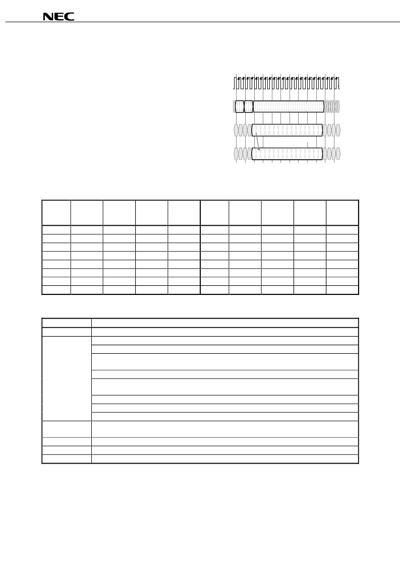
Figure 20-1 SETR, CLRR, SETF Transaction
SCK
CMD
SIO0
T
20
SRQ packet - SETR/CLRR/SETF
1111
00000000...00000000
SRQ packet - SETR/CLRR/SETF
0000
SIO1
T
4
The packet is repeated
from SIO0 to SIO1
1
1
1
1
0
0
0
0
相關(guān)PDF資料 |
PDF描述 |
|---|---|
| UPD488448FB-C80-45-DQ2 | 128 M-bit Direct Rambus⑩ DRAM |
| UPD488448FB-C71-45-DQ1 | 128 M-bit Direct Rambus⑩ DRAM |
| UPD488448FB-C71-45-DQ2 | 128 M-bit Direct Rambus⑩ DRAM |
| UPD488448FB-C60-53-DQ2 | 128 M-bit Direct Rambus⑩ DRAM |
| UPD488448FF-C80-45-DQ1 | 128 M-bit Direct Rambus⑩ DRAM |
相關(guān)代理商/技術(shù)參數(shù) |
參數(shù)描述 |
|---|---|
| UPD4990AG-A | 制造商:Renesas Electronics 功能描述:Cut Tape |
| UPD4991ACX-A | 制造商:Renesas Electronics Corporation 功能描述: |
| UPD4992CX-A | 制造商:Renesas Electronics 功能描述:Cut Tape |
| UPD50256CP15 | 制造商:HIT 功能描述:50256 HITACHI'86 SMT N9F8A |
| UPD50256CP-15 | 制造商:HIT 功能描述:50256 HITACHI'86 SMT N9F8A |
發(fā)布緊急采購(gòu),3分鐘左右您將得到回復(fù)。