- 您現(xiàn)在的位置:買(mǎi)賣(mài)IC網(wǎng) > PDF目錄358635 > 38D5 (Renesas Technology Corp.) SINGLE-CHIP 8-BIT CMOS MICROCOMPUTER PDF資料下載
參數(shù)資料
| 型號(hào): | 38D5 |
| 廠商: | Renesas Technology Corp. |
| 英文描述: | SINGLE-CHIP 8-BIT CMOS MICROCOMPUTER |
| 中文描述: | 單芯片8位CMOS微機(jī) |
| 文件頁(yè)數(shù): | 129/141頁(yè) |
| 文件大小: | 2027K |
| 代理商: | 38D5 |
第1頁(yè)第2頁(yè)第3頁(yè)第4頁(yè)第5頁(yè)第6頁(yè)第7頁(yè)第8頁(yè)第9頁(yè)第10頁(yè)第11頁(yè)第12頁(yè)第13頁(yè)第14頁(yè)第15頁(yè)第16頁(yè)第17頁(yè)第18頁(yè)第19頁(yè)第20頁(yè)第21頁(yè)第22頁(yè)第23頁(yè)第24頁(yè)第25頁(yè)第26頁(yè)第27頁(yè)第28頁(yè)第29頁(yè)第30頁(yè)第31頁(yè)第32頁(yè)第33頁(yè)第34頁(yè)第35頁(yè)第36頁(yè)第37頁(yè)第38頁(yè)第39頁(yè)第40頁(yè)第41頁(yè)第42頁(yè)第43頁(yè)第44頁(yè)第45頁(yè)第46頁(yè)第47頁(yè)第48頁(yè)第49頁(yè)第50頁(yè)第51頁(yè)第52頁(yè)第53頁(yè)第54頁(yè)第55頁(yè)第56頁(yè)第57頁(yè)第58頁(yè)第59頁(yè)第60頁(yè)第61頁(yè)第62頁(yè)第63頁(yè)第64頁(yè)第65頁(yè)第66頁(yè)第67頁(yè)第68頁(yè)第69頁(yè)第70頁(yè)第71頁(yè)第72頁(yè)第73頁(yè)第74頁(yè)第75頁(yè)第76頁(yè)第77頁(yè)第78頁(yè)第79頁(yè)第80頁(yè)第81頁(yè)第82頁(yè)第83頁(yè)第84頁(yè)第85頁(yè)第86頁(yè)第87頁(yè)第88頁(yè)第89頁(yè)第90頁(yè)第91頁(yè)第92頁(yè)第93頁(yè)第94頁(yè)第95頁(yè)第96頁(yè)第97頁(yè)第98頁(yè)第99頁(yè)第100頁(yè)第101頁(yè)第102頁(yè)第103頁(yè)第104頁(yè)第105頁(yè)第106頁(yè)第107頁(yè)第108頁(yè)第109頁(yè)第110頁(yè)第111頁(yè)第112頁(yè)第113頁(yè)第114頁(yè)第115頁(yè)第116頁(yè)第117頁(yè)第118頁(yè)第119頁(yè)第120頁(yè)第121頁(yè)第122頁(yè)第123頁(yè)第124頁(yè)第125頁(yè)第126頁(yè)第127頁(yè)第128頁(yè)當(dāng)前第129頁(yè)第130頁(yè)第131頁(yè)第132頁(yè)第133頁(yè)第134頁(yè)第135頁(yè)第136頁(yè)第137頁(yè)第138頁(yè)第139頁(yè)第140頁(yè)第141頁(yè)
Rev.3.01
REJ03B0158-0301
Aug 08, 2007
Page 129 of 134
38D5 Group
Notes on LCD Drive Control Circuit
1. Multiplier Circuit
When the multiplier circuit is used, set the multiplier circuit
control bit to “1” (multiplier circuit enabled) after applying a
voltage from 1.3 V or more to 2.1 V or less to the V
L1
pin.
When the multiplier circuit is not used, set the V
L3
connection bit
to “1” (open) and apply an appropriate voltage to the LCD power
source input pins (V
L1
to V
L3
). When the V
L3
connection bit is
set open, the V
L3
pin is placed in the high impedance state.
When the multiplier circuit is used, set the LCDCK frequency to
100 Hz or more. The on-chip oscillator cannot be used as
LCDCK.
In a system where the multiplier circuit is used (a multiplier
capacitor is externally connected between the C
1
and C
2
pins),
set the multiplier circuit control bit to “1” (multiplier circuit
enabled) before executing the STP or WIT instruction.
2. Setting Data to LCD Display RAM
To write data to the LCD display RAM when the LCD enable bit
is set to “1” and while LCD is turned on, set fixed data.
Rewriting with temporary data may cause LCD to flicker. The
following shows a processing example to write data to the LCD
display RAM while LCD is turned on.
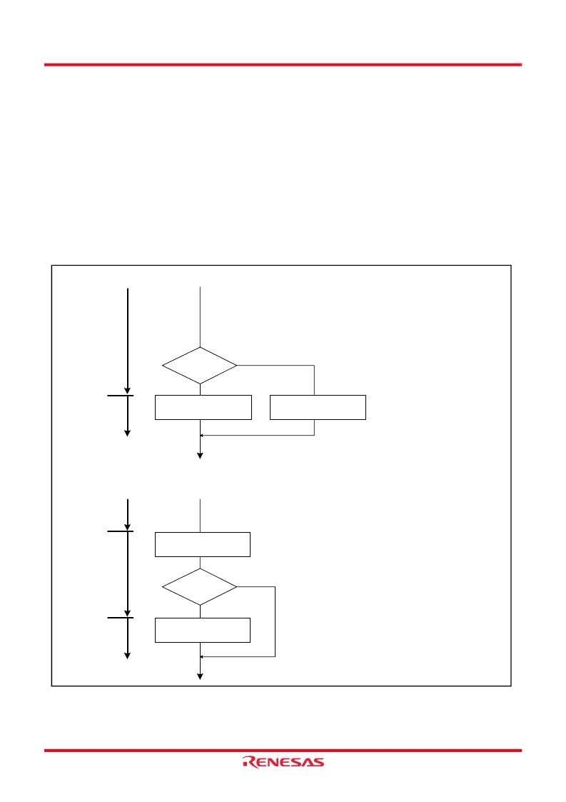
Fig. 105 Processing example when writing data to LCD display RAM While LCD Turned On
(1) Ccorrect processing
LCD
on
LCD
on or
off
*Content at address 0840
16
: “FF
16
”
Off
On
Set LCD display RAM data
LRAM0 (address 0840
16
)
←
“FF
16
”
LCD on or off
Set LCD display RAM data
LRAM0 (address 0840
16
)
←
“00
16
”
Set fixed data to LCD display RAM
(2) Incorrect processing
LCD
on
LCD
on or
off
*Content at address 0840
16
: “FF
16
”
Off
On
Set LCD display RAM data
LRAM0 (address 0840
16
)
←
“FF
16
”
LCD on or off
Set LCD display RAM data
LRAM0 (address 0840
16
)
←
“00
16
”
Set off data to LCD display RAM
LCD
off
Set fixed data to LCD display RAM
相關(guān)PDF資料 |
PDF描述 |
|---|---|
| 38F1222 | 300mA LDO Linear Regulators with Internal Microprocessor Reset Circuit |
| TA5M | STECKER DIN MINI 5POL |
| 70B5031 | KUPPLUNG DIN MINI 5POL |
| 39-26-3050 | 300mA LDO Linear Regulators with Internal Microprocessor Reset Circuit |
| 390KD05JX | 11 to 460 Volts Varistor 0.7 to 29 Joule |
相關(guān)代理商/技術(shù)參數(shù) |
參數(shù)描述 |
|---|---|
| 38D5_07 | 制造商:RENESAS 制造商全稱:Renesas Technology Corp 功能描述:Standard Characteristics Example |
| 38D5_08 | 制造商:RENESAS 制造商全稱:Renesas Technology Corp 功能描述:SINGLE-CHIP 8-BIT CMOS MICROCOMPUTER |
| 38D511G015FE6AD | 制造商:Sprague/Vishay 功能描述:AL015X751 |
| 38D5-FMV | 制造商:RENESAS 制造商全稱:Renesas Technology Corp 功能描述:Standard Characteristics (Flash Memory Version) |
| 38DDP11B11M1QT | 功能描述:SWITCH PUSH DPDT,O-N-O,N,SL,LF , 制造商:grayhill inc. 系列:* 零件狀態(tài):在售 標(biāo)準(zhǔn)包裝:1 |
發(fā)布緊急采購(gòu),3分鐘左右您將得到回復(fù)。