- 您現(xiàn)在的位置:買賣IC網(wǎng) > PDF目錄369945 > P8XC591 (NXP Semiconductors N.V.) HiRel FPGA, Low-Power 1.0?? CMOS Technology PDF資料下載
參數(shù)資料
| 型號(hào): | P8XC591 |
| 廠商: | NXP Semiconductors N.V. |
| 英文描述: | HiRel FPGA, Low-Power 1.0?? CMOS Technology |
| 中文描述: | 單芯片8 - CAN控制器位微控制器 |
| 文件頁(yè)數(shù): | 80/160頁(yè) |
| 文件大小: | 601K |
| 代理商: | P8XC591 |
第1頁(yè)第2頁(yè)第3頁(yè)第4頁(yè)第5頁(yè)第6頁(yè)第7頁(yè)第8頁(yè)第9頁(yè)第10頁(yè)第11頁(yè)第12頁(yè)第13頁(yè)第14頁(yè)第15頁(yè)第16頁(yè)第17頁(yè)第18頁(yè)第19頁(yè)第20頁(yè)第21頁(yè)第22頁(yè)第23頁(yè)第24頁(yè)第25頁(yè)第26頁(yè)第27頁(yè)第28頁(yè)第29頁(yè)第30頁(yè)第31頁(yè)第32頁(yè)第33頁(yè)第34頁(yè)第35頁(yè)第36頁(yè)第37頁(yè)第38頁(yè)第39頁(yè)第40頁(yè)第41頁(yè)第42頁(yè)第43頁(yè)第44頁(yè)第45頁(yè)第46頁(yè)第47頁(yè)第48頁(yè)第49頁(yè)第50頁(yè)第51頁(yè)第52頁(yè)第53頁(yè)第54頁(yè)第55頁(yè)第56頁(yè)第57頁(yè)第58頁(yè)第59頁(yè)第60頁(yè)第61頁(yè)第62頁(yè)第63頁(yè)第64頁(yè)第65頁(yè)第66頁(yè)第67頁(yè)第68頁(yè)第69頁(yè)第70頁(yè)第71頁(yè)第72頁(yè)第73頁(yè)第74頁(yè)第75頁(yè)第76頁(yè)第77頁(yè)第78頁(yè)第79頁(yè)當(dāng)前第80頁(yè)第81頁(yè)第82頁(yè)第83頁(yè)第84頁(yè)第85頁(yè)第86頁(yè)第87頁(yè)第88頁(yè)第89頁(yè)第90頁(yè)第91頁(yè)第92頁(yè)第93頁(yè)第94頁(yè)第95頁(yè)第96頁(yè)第97頁(yè)第98頁(yè)第99頁(yè)第100頁(yè)第101頁(yè)第102頁(yè)第103頁(yè)第104頁(yè)第105頁(yè)第106頁(yè)第107頁(yè)第108頁(yè)第109頁(yè)第110頁(yè)第111頁(yè)第112頁(yè)第113頁(yè)第114頁(yè)第115頁(yè)第116頁(yè)第117頁(yè)第118頁(yè)第119頁(yè)第120頁(yè)第121頁(yè)第122頁(yè)第123頁(yè)第124頁(yè)第125頁(yè)第126頁(yè)第127頁(yè)第128頁(yè)第129頁(yè)第130頁(yè)第131頁(yè)第132頁(yè)第133頁(yè)第134頁(yè)第135頁(yè)第136頁(yè)第137頁(yè)第138頁(yè)第139頁(yè)第140頁(yè)第141頁(yè)第142頁(yè)第143頁(yè)第144頁(yè)第145頁(yè)第146頁(yè)第147頁(yè)第148頁(yè)第149頁(yè)第150頁(yè)第151頁(yè)第152頁(yè)第153頁(yè)第154頁(yè)第155頁(yè)第156頁(yè)第157頁(yè)第158頁(yè)第159頁(yè)第160頁(yè)
2000 Jul 26
80
Philips Semiconductors
Preliminary Specification
Single-chip 8-bit microcontroller with CAN controller
P8xC591
15.2.10.1 The Address Register, S1ADR
The CPU can read from and write to this 8-bit, directly
addressable SFR. S1ADR is not affected by the SIO1
hardware. The contents of this register are irrelevant when
SIO1 is in a master mode. In the slave modes, the seven
most significant bits must be loaded with the
microcontrollers own slave address, and, if the least
significant bit is set, the general call address (00H) is
recognized; otherwise it is ignored.
Themostsignificantbitcorrespondstothefirstbitreceived
from the I
2
C bus after a start condition. A logic 1 in S1ADR
corresponds to a high level on the I
2
C bus, and a logic 0
corresponds to a low level on the bus.
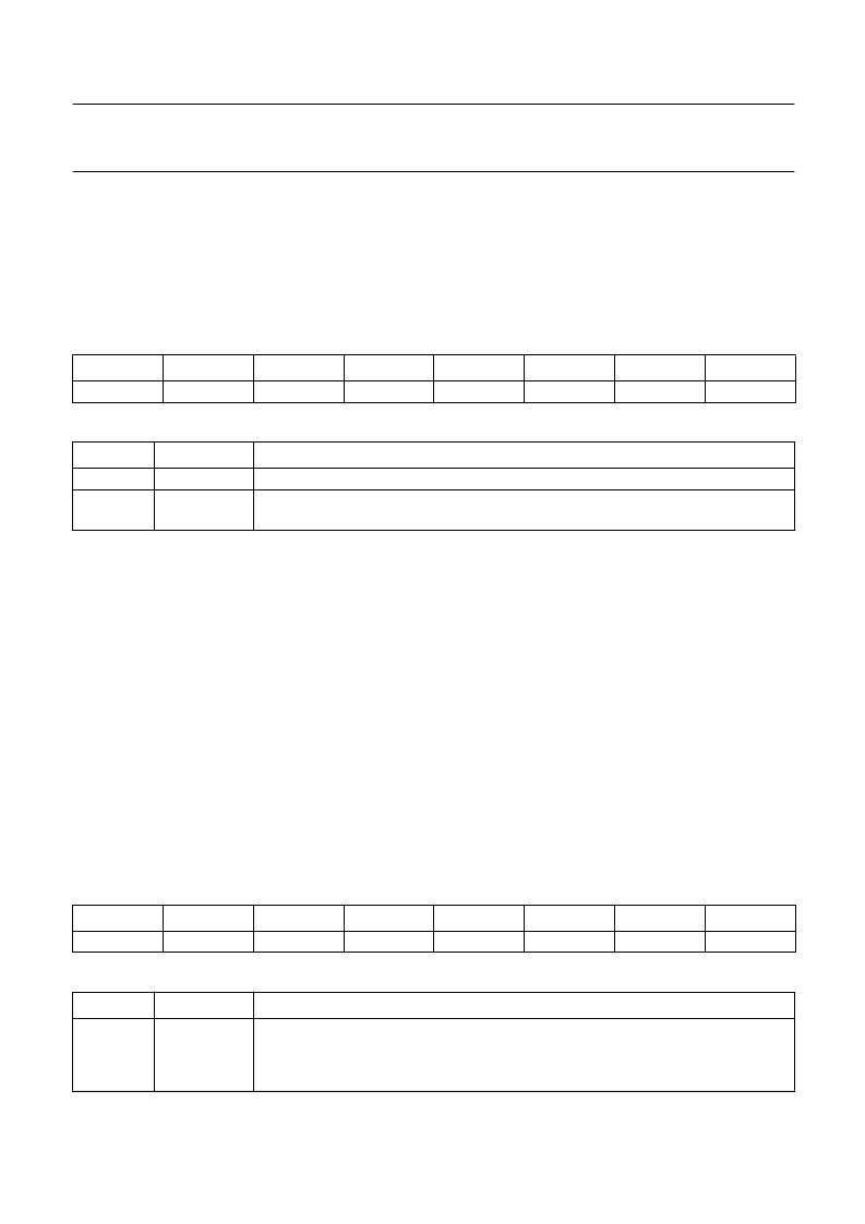
Table 51
Address Register S1ADR (address DBH)
Table 52
Description of S1ADR (DBH) bits
7
6
5
4
3
2
1
0
X
X
X
X
X
X
X
GC
BIT
SYMBOL
DESCRIPTION
7 to 1
0
X
Own slave address.
0 = general call address is not recognized.
1 = general call address is recognized.
GC
15.2.11 T
HE
D
ATA
R
EGISTER
, S1DAT
S1DAT contains a byte of serial data to be transmitted or
a byte which has just been received. The CPU can read
from and write to this 8-bit, directly addressable SFR while
it is not in the process of shifting a byte. This occurs when
SIO1 is in a defined state and the serial interrupt flag is set.
Data in S1DAT remains stable as long as SI is set. Data in
S1DAT is always shifted from right to left: the first bit to be
transmitted is the MSB (bit 7), and, after a byte has been
received, the first bit of received data is located at the MSB
of S1DAT. While data is being shifted out, data on the bus
is simultaneously being shifted in; S1DAT always contains
the last data byte present on the bus. Thus, in the event of
lost arbitration, the transition from master transmitter to
slave receiver is made with the correct data in S1DAT.
S1DAT and the ACK flag form a 9-bit shift register which
shifts in or shifts out an 8-bit byte, followed by an
acknowledge bit. The ACK flag is controlled by the SIO1
hardwareand cannotbeaccessedbytheCPU. Serialdata
is shifted through the ACK flag into S1DAT on the rising
edges of serial clock pulses on the SCL line. When a byte
has been shifted into S1DAT, the serial data is available in
S1DAT, and the acknowledge bit is returned by the control
logic during the ninth clock pulse. Serial data is shifted out
from S1DAT via a buffer (BSD7) on the falling edges of
clock pulses on the SCL line.
When the CPU writes to S1DAT, BSD7 is loaded with the
content of S1DAT.7, which is the first bit to be transmitted
to the SDA line (see Figure 36). After nine serial clock
pulses, the eight bits in S1DAT will have been transmitted
to the SDA line, and the acknowledge bit will be present in
ACK. Note that the eight transmitted bits are shifted back
into S1DAT.
Table 53
Address Register S1DAT (address DAH)
Table 54
Description of S1DAT (DAH) bits
7
6
5
4
3
2
1
0
SD7
SD6
SD5
SD4
SD3
SD2
SD1
SD0
BIT
SYMBOL
DESCRIPTION
7 to 0
SD7 to SD0
Eight bits to be transmitted or just received. A logic 1 in S1DAT corresponds to a high
level on the I
2
C bus, and a logic 0 corresponds to a low level on the bus. Serial data
shifts through S1DAT from right to left. Figure 35 shows how data in S1DAT is serially
transferred to and from the SDA line.
相關(guān)PDF資料 |
PDF描述 |
|---|---|
| P90CE201 | 16-bit microcontroller |
| P90CE201AEB | 16-bit microcontroller |
| P9217 | PbS photoconductive detector |
| P930 | CdS photoconductive cell |
| PA025XSB | This technical specification applies to 2.5inch color TFT-LCD panel. |
相關(guān)代理商/技術(shù)參數(shù) |
參數(shù)描述 |
|---|---|
| P8XC592 | 制造商:PHILIPS 制造商全稱:NXP Semiconductors 功能描述:8-bit microcontroller with on-chip CAN |
| P8XCE598 | 制造商:PHILIPS 制造商全稱:NXP Semiconductors 功能描述:8-bit microcontroller with on-chip CAN |
| P8XCL580HFH | 制造商:PHILIPS 制造商全稱:NXP Semiconductors 功能描述:Low voltage 8-bit microcontrollers with UART, I2C-bus and ADC |
| P8XCL580HFT | 制造商:PHILIPS 制造商全稱:NXP Semiconductors 功能描述:Low voltage 8-bit microcontrollers with UART, I2C-bus and ADC |
| P8Z77 DELUXE | 制造商:Asus 功能描述:P8Z77-V Deluxe ATX Motherboard |
發(fā)布緊急采購(gòu),3分鐘左右您將得到回復(fù)。