- 您現(xiàn)在的位置:買賣IC網(wǎng) > PDF目錄16537 > AD9558/PCBZ (Analog Devices Inc)BOARD EVAL FOR AD9558 PDF資料下載
參數(shù)資料
| 型號(hào): | AD9558/PCBZ |
| 廠商: | Analog Devices Inc |
| 文件頁數(shù): | 50/104頁 |
| 文件大?。?/td> | 0K |
| 描述: | BOARD EVAL FOR AD9558 |
| 產(chǎn)品變化通告: | AD9558 Minor Metal Mask Change 17/Apr/2012 |
| 設(shè)計(jì)資源: | AD9558 Eval Brd BOM AD9558 Schematic |
| 標(biāo)準(zhǔn)包裝: | 1 |
| 系列: | * |
第1頁第2頁第3頁第4頁第5頁第6頁第7頁第8頁第9頁第10頁第11頁第12頁第13頁第14頁第15頁第16頁第17頁第18頁第19頁第20頁第21頁第22頁第23頁第24頁第25頁第26頁第27頁第28頁第29頁第30頁第31頁第32頁第33頁第34頁第35頁第36頁第37頁第38頁第39頁第40頁第41頁第42頁第43頁第44頁第45頁第46頁第47頁第48頁第49頁當(dāng)前第50頁第51頁第52頁第53頁第54頁第55頁第56頁第57頁第58頁第59頁第60頁第61頁第62頁第63頁第64頁第65頁第66頁第67頁第68頁第69頁第70頁第71頁第72頁第73頁第74頁第75頁第76頁第77頁第78頁第79頁第80頁第81頁第82頁第83頁第84頁第85頁第86頁第87頁第88頁第89頁第90頁第91頁第92頁第93頁第94頁第95頁第96頁第97頁第98頁第99頁第100頁第101頁第102頁第103頁第104頁
Data Sheet
AD9558
Rev. B | Page 5 of 104
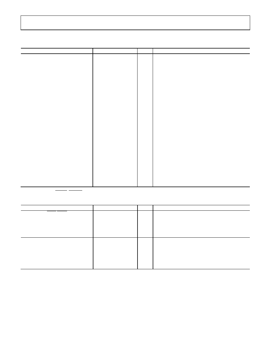
POWER DISSIPATION
Table 3.
Parameter
Min
Typ
Max
Unit
Test Conditions/Comments
POWER DISSIPATION
Typical Configuration
0.47
0.74
1.02
W
System clock: 49.152 MHz crystal; DPLL active;
both 19.44 MHz input references in differential mode;
one HSTL driver at 644.53125 MHz;
one 3.3 V CMOS driver at 161.1328125 MHz and 80 pF
capacitive load on CMOS output
All Blocks Running
0.6
1.0
1.32
W
System clock: 49.152 MHz crystal; DPLL active;
both input references in differential mode;
four HSTL drivers at 750 MHz;
four 3.3 V CMOS drivers at 250 MHz and 80 pF capacitive
load on CMOS outputs
Full Power-Down
44
125
mW
Typical configuration with no external pull-up or pull-
down resistors; about 2/3 of this power is on AVDD3
Incremental Power Dissipation
Conditions = typical configuration; table values show the
change in power due to the indicated operation
Input Reference On/Off
Differential Without Divide-by-2
20
25
32
mW
Additional current draw is in the DVDD3 domain only
Differential With Divide-by-2
26
32
40
mW
Additional current draw is in the DVDD3 domain only
Single-Ended (Without Divide-by-2)
5
7
9
mW
Additional current draw is in the DVDD3 domain only
Output Distribution Driver On/Off
LVDS (at 750 MHz)
12
17
22
mW
Additional current draw is in the AVDD domain only
HSTL (at 750 MHz)
14
21
28
mW
Additional current draw is in the AVDD domain only
1.8 V CMOS (at 250 MHz)
14
21
28
mW
A single 1.8 V CMOS output with an 80 pF load
3.3 V CMOS (at 250 MHz)
18
27
36
mW
A single 3.3 V CMOS output with an 80 pF load
Other Blocks On/Off
Second RF Divider
36
51
64
mW
Additional current draw is in the AVDD domain only
Channel Divider Bypassed
10
17
23
mW
Additional current draw is in the AVDD domain only
LOGIC INPUTS (SYNC
E
, RESET, PINCONTROL,
A
M7 TO M0
A
)
Table 4.
Parameter
Min
Typ
Max
Unit
Test Conditions/Comments
LOGIC INPUTS (
AA
SYNC
EEAA
,
A
RESETE
A
, PINCONTROL)
Input High Voltage (VIH)
2.1
V
Input Low Voltage (VIL)
0.8
V
Input Current (IINH, IINL)
±50
±100
A
Input Capacitance (CIN)
3
pF
LOGIC INPUTS (M7 to M0)
Input High Voltage (VIH)
2.5
V
Input Level Voltage (VIM)
1.0
2.2
V
Input Low Voltage (VIL)
0.6
V
Input Current (IINH, IINL)
±60
±100
A
Input Capacitance (CIN)
3
pF
相關(guān)PDF資料 |
PDF描述 |
|---|---|
| GBM22DSAH | CONN EDGECARD 44POS R/A .156 SLD |
| DK-2632-03 | CABLE FIBER OPTIC DUAL LC-SC 3M |
| GEM30DTAS | CONN EDGECARD 60POS R/A .156 SLD |
| GMM12DRXI | CONN EDGECARD 24POS DIP .156 SLD |
| P1330R-105K | INDUCTOR POWER 1000.0UH SMD |
相關(guān)代理商/技術(shù)參數(shù) |
參數(shù)描述 |
|---|---|
| AD9559 | 制造商:AD 制造商全稱:Analog Devices 功能描述:Dual PLL, Quad Input, Multiservice Line Card Adaptive Clock Translator |
| AD9559/PCBZ | 功能描述:時(shí)鐘和定時(shí)器開發(fā)工具 Multi-protocol line card dual clock RoHS:否 制造商:Texas Instruments 產(chǎn)品:Evaluation Modules 類型:Clock Conditioners 工具用于評(píng)估:LMK04100B 頻率:122.8 MHz 工作電源電壓:3.3 V |
| AD9559BCPZ | 功能描述:時(shí)鐘發(fā)生器及支持產(chǎn)品 Multi-protocol line card dual clock RoHS:否 制造商:Silicon Labs 類型:Clock Generators 最大輸入頻率:14.318 MHz 最大輸出頻率:166 MHz 輸出端數(shù)量:16 占空比 - 最大:55 % 工作電源電壓:3.3 V 工作電源電流:1 mA 最大工作溫度:+ 85 C 安裝風(fēng)格:SMD/SMT 封裝 / 箱體:QFN-56 |
| AD9559BCPZ-REEL7 | 功能描述:時(shí)鐘發(fā)生器及支持產(chǎn)品 Multi-protocol line card dual clock RoHS:否 制造商:Silicon Labs 類型:Clock Generators 最大輸入頻率:14.318 MHz 最大輸出頻率:166 MHz 輸出端數(shù)量:16 占空比 - 最大:55 % 工作電源電壓:3.3 V 工作電源電流:1 mA 最大工作溫度:+ 85 C 安裝風(fēng)格:SMD/SMT 封裝 / 箱體:QFN-56 |
| AD9559PCBZ | 制造商:AD 制造商全稱:Analog Devices 功能描述:Dual PLL, Quad Input, Multiservice Line Card Adaptive Clock Translator |
發(fā)布緊急采購,3分鐘左右您將得到回復(fù)。