- 您現(xiàn)在的位置:買賣IC網(wǎng) > PDF目錄97869 > DS3131 (MAXIM INTEGRATED PRODUCTS INC) SPECIALTY TELECOM CIRCUIT, PBGA256 PDF資料下載
參數(shù)資料
| 型號(hào): | DS3131 |
| 廠商: | MAXIM INTEGRATED PRODUCTS INC |
| 元件分類: | Telecom IC:Other |
| 英文描述: | SPECIALTY TELECOM CIRCUIT, PBGA256 |
| 封裝: | 27 X 27 MM, PLASTIC, BGA-256 |
| 文件頁數(shù): | 24/174頁 |
| 文件大小: | 1261K |
| 代理商: | DS3131 |
第1頁第2頁第3頁第4頁第5頁第6頁第7頁第8頁第9頁第10頁第11頁第12頁第13頁第14頁第15頁第16頁第17頁第18頁第19頁第20頁第21頁第22頁第23頁當(dāng)前第24頁第25頁第26頁第27頁第28頁第29頁第30頁第31頁第32頁第33頁第34頁第35頁第36頁第37頁第38頁第39頁第40頁第41頁第42頁第43頁第44頁第45頁第46頁第47頁第48頁第49頁第50頁第51頁第52頁第53頁第54頁第55頁第56頁第57頁第58頁第59頁第60頁第61頁第62頁第63頁第64頁第65頁第66頁第67頁第68頁第69頁第70頁第71頁第72頁第73頁第74頁第75頁第76頁第77頁第78頁第79頁第80頁第81頁第82頁第83頁第84頁第85頁第86頁第87頁第88頁第89頁第90頁第91頁第92頁第93頁第94頁第95頁第96頁第97頁第98頁第99頁第100頁第101頁第102頁第103頁第104頁第105頁第106頁第107頁第108頁第109頁第110頁第111頁第112頁第113頁第114頁第115頁第116頁第117頁第118頁第119頁第120頁第121頁第122頁第123頁第124頁第125頁第126頁第127頁第128頁第129頁第130頁第131頁第132頁第133頁第134頁第135頁第136頁第137頁第138頁第139頁第140頁第141頁第142頁第143頁第144頁第145頁第146頁第147頁第148頁第149頁第150頁第151頁第152頁第153頁第154頁第155頁第156頁第157頁第158頁第159頁第160頁第161頁第162頁第163頁第164頁第165頁第166頁第167頁第168頁第169頁第170頁第171頁第172頁第173頁第174頁
DS3131
12 of 174
Restrictions
In creating the overall system architecture, the user must balance the port, throughput, and HDLC
channel restrictions of the DS3131. Table 2-A lists all of the upper-bound maximum restrictions.
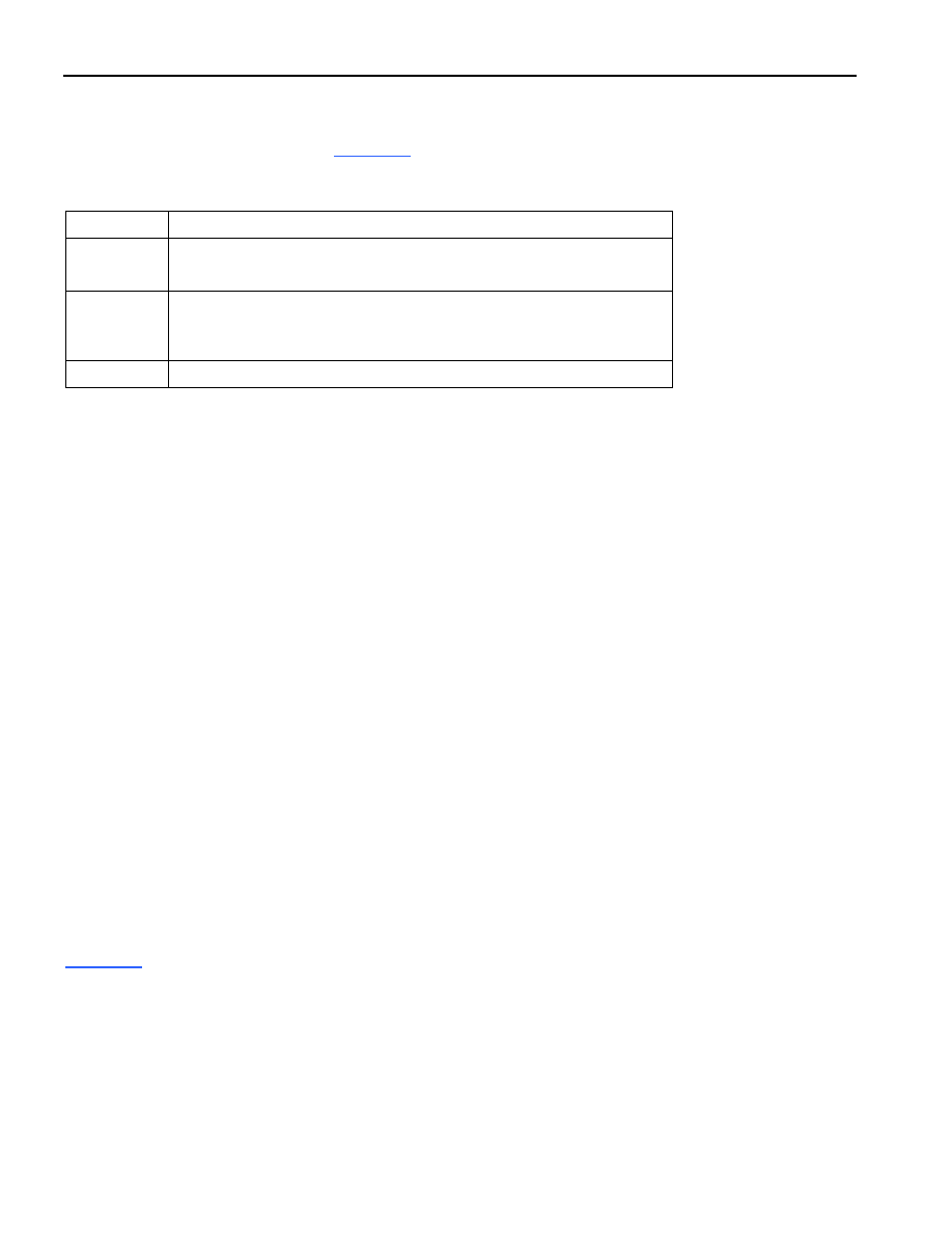
Table 2-A. Restrictions
ITEM
RESTRICTION
Maximum of 40 physical ports
Port
Maximum data rate of 52Mbps
Maximum receive: 132Mbps (Refer to Application Note 358: DS3134
PCI Bus Utilization.)
Throughput
Maximum transmit: 132Mbps
HDLC
Maximum of 40 channels
Internal Device Configuration Registers
All internal device configuration registers (with the exception of the PCI configuration registers, which
are 32-bit registers) are 16 bits wide and are not byte addressable. When the host on the PCI bus accesses
these registers, the particular combination of byte enables (i.e., PCBE signals) is not important, but at
least one of the byte enables must be asserted for a transaction to occur. All registers are read/write,
unless otherwise noted. Reserved bits should not be modified to allow for future upgrades to the device.
These bits should be treated as having no meaning and could be either 0 or 1 when read.
Initialization
On a system reset (which can be invoked by either hardware action through the PRST signal or software
action through the RST control bit in the master reset and ID register), all of the internal device
configuration registers are set to 0 (0000h). The local bus bridge mode control register (LBBMC) is not
affected by a software-invoked system reset; it is forced to all zeros only by a hardware reset. The
internal registers that are accessed indirectly (these are listed as “indirect registers” in the data sheet and
consist of the port DS0 configuration registers in the Layer 1 block, the DMA configuration RAMs, and
the FIFO registers) are not affected by a system reset, so they must be configured on power-up by the
host to a proper state.
By design, the DS3131 BoSS does not take control of the PCI bus upon power-up. All physical ports
start up by sending all ones (not the HDLC idle code), so the BoSS is idle upon power-up. Please note,
however, that the BoSS uses internal RAM to periodically store and retrieve the states of the internal
state machines. Because there are many such complex state machines and interworking functional blocks
inside the BoSS, all internal registers must be initialized to a known state before any data packets can be
transmitted and received.
Table 2-B lists the steps required to initialize the DS3131. It is imperative that they are followed exactly
in the order presented, or exactly as implemented in Dallas Semiconductor DS3131 driver code.
相關(guān)PDF資料 |
PDF描述 |
|---|---|
| DS3134 | DATACOM, FRAMER, PBGA256 |
| DS3150QN | DATACOM, PCM TRANSCEIVER, PQCC28 |
| DS3150Q | DATACOM, PCM TRANSCEIVER, PQCC28 |
| DS3150TN | DATACOM, PCM TRANSCEIVER, PDIP48 |
| DS3150T | DATACOM, PCM TRANSCEIVER, PQFP48 |
相關(guān)代理商/技術(shù)參數(shù) |
參數(shù)描述 |
|---|---|
| DS3131DK | 功能描述:通信集成電路 - 若干 RoHS:否 制造商:Maxim Integrated 類型:Transport Devices 封裝 / 箱體:TECSBGA-256 數(shù)據(jù)速率:100 Mbps 電源電壓-最大:1.89 V, 3.465 V 電源電壓-最小:1.71 V, 3.135 V 電源電流:50 mA, 225 mA 最大工作溫度:+ 85 C 最小工作溫度:- 40 C 封裝:Tube |
| DS3134 | 功能描述:IC CTRLR HDLC CHATEAU 256-BGA RoHS:否 類別:集成電路 (IC) >> 接口 - 控制器 系列:- 標(biāo)準(zhǔn)包裝:4,900 系列:- 控制器類型:USB 2.0 控制器 接口:串行 電源電壓:3 V ~ 3.6 V 電流 - 電源:135mA 工作溫度:0°C ~ 70°C 安裝類型:表面貼裝 封裝/外殼:36-VFQFN 裸露焊盤 供應(yīng)商設(shè)備封裝:36-QFN(6x6) 包裝:* 其它名稱:Q6396337A |
| DS-313PIN | 制造商:未知廠家 制造商全稱:未知廠家 功能描述:Analog Miscellaneous |
| DS-313-PIN | 功能描述:信號(hào)調(diào)節(jié) RoHS:否 制造商:EPCOS 產(chǎn)品:Duplexers 頻率:782 MHz, 751 MHz 頻率范圍: 電壓額定值: 帶寬: 阻抗:50 Ohms 端接類型:SMD/SMT 封裝 / 箱體:2.5 mm x 2 mm 工作溫度范圍:- 30 C to + 85 C 封裝:Reel |
| DS31400 | 制造商:MAXIM 制造商全稱:Maxim Integrated Products 功能描述:8-Input, 14-Output, Dual DPLL Timing IC with Sub-ps Output Jitter |
發(fā)布緊急采購,3分鐘左右您將得到回復(fù)。