- 您現(xiàn)在的位置:買賣IC網(wǎng) > PDF目錄378055 > PM6344 (PMC-SIERRA INC) Ultraframer DS3/E3/DS2/E2/DS1/E1/DS0 PDF資料下載
參數(shù)資料
| 型號: | PM6344 |
| 廠商: | PMC-SIERRA INC |
| 元件分類: | 數(shù)字傳輸電路 |
| 英文描述: | Ultraframer DS3/E3/DS2/E2/DS1/E1/DS0 |
| 中文描述: | DATACOM, FRAMER, PQFP128 |
| 封裝: | 20 X 14 MM, PLASTIC, QFP-128 |
| 文件頁數(shù): | 194/256頁 |
| 文件大小: | 1030K |
| 代理商: | PM6344 |
第1頁第2頁第3頁第4頁第5頁第6頁第7頁第8頁第9頁第10頁第11頁第12頁第13頁第14頁第15頁第16頁第17頁第18頁第19頁第20頁第21頁第22頁第23頁第24頁第25頁第26頁第27頁第28頁第29頁第30頁第31頁第32頁第33頁第34頁第35頁第36頁第37頁第38頁第39頁第40頁第41頁第42頁第43頁第44頁第45頁第46頁第47頁第48頁第49頁第50頁第51頁第52頁第53頁第54頁第55頁第56頁第57頁第58頁第59頁第60頁第61頁第62頁第63頁第64頁第65頁第66頁第67頁第68頁第69頁第70頁第71頁第72頁第73頁第74頁第75頁第76頁第77頁第78頁第79頁第80頁第81頁第82頁第83頁第84頁第85頁第86頁第87頁第88頁第89頁第90頁第91頁第92頁第93頁第94頁第95頁第96頁第97頁第98頁第99頁第100頁第101頁第102頁第103頁第104頁第105頁第106頁第107頁第108頁第109頁第110頁第111頁第112頁第113頁第114頁第115頁第116頁第117頁第118頁第119頁第120頁第121頁第122頁第123頁第124頁第125頁第126頁第127頁第128頁第129頁第130頁第131頁第132頁第133頁第134頁第135頁第136頁第137頁第138頁第139頁第140頁第141頁第142頁第143頁第144頁第145頁第146頁第147頁第148頁第149頁第150頁第151頁第152頁第153頁第154頁第155頁第156頁第157頁第158頁第159頁第160頁第161頁第162頁第163頁第164頁第165頁第166頁第167頁第168頁第169頁第170頁第171頁第172頁第173頁第174頁第175頁第176頁第177頁第178頁第179頁第180頁第181頁第182頁第183頁第184頁第185頁第186頁第187頁第188頁第189頁第190頁第191頁第192頁第193頁當(dāng)前第194頁第195頁第196頁第197頁第198頁第199頁第200頁第201頁第202頁第203頁第204頁第205頁第206頁第207頁第208頁第209頁第210頁第211頁第212頁第213頁第214頁第215頁第216頁第217頁第218頁第219頁第220頁第221頁第222頁第223頁第224頁第225頁第226頁第227頁第228頁第229頁第230頁第231頁第232頁第233頁第234頁第235頁第236頁第237頁第238頁第239頁第240頁第241頁第242頁第243頁第244頁第245頁第246頁第247頁第248頁第249頁第250頁第251頁第252頁第253頁第254頁第255頁第256頁
STANDARD PRODUCT
PMC-Sierra, Inc.
PM6344 EQUAD
PMC-951013
ISSUE 5
QUADRUPLE E1 FRAMER
181
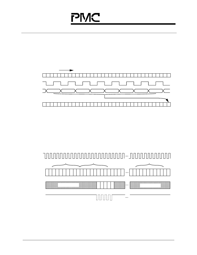
range between 4 bit/s and 20 kbit/s. RDLSIG[x] is generated on the falling edge
of RDLCLK[x]. For the diagram shown above, the SRSMFP and SRCMFP
register bits are set to logic 0. The timing with respect to RCLKO[x] shown here
is valid only if the RCLKOSEL bit is set to logic 0.
Figure 11
- TS16 Transmit Datalink Interface
TDLCLK[x]
TDLSIG[x]
TDP/TDD[x]
TDN[x]
Bit 1
Bit 2
Bit 3
Bit 4
Bit 5
Bit 6
Bit 7
Bit 8
1
2
3
4
5
6
7
0
8
9
10 11 12 13 14 15 16
15 16 17 18 19 20 21 22 23 24 25 26 27 28 29 30 31
14
Time Slots
BTPCM[x]
15 16 17 18 19 20 21 22 23 24 25 26 27 28 29 30 31
1
2
3
4
5
6
7
0
8
9
10 11 12 13 14 15 16 17
CCS data collected over 32 timeslots
and inserted into TS16
When Common Channel Signaling (CCS) data sourced from TDLSIG[x] is
selected (DLEN=1, SIGEN=0 and TXDMASIG=0), TDLCLK[x] is active,
producing one cycle every 4 time slots, aligned to the incoming BTPCM[x]. The
data on TDLSIG[x] is sampled on the rising edge of TDLCLK[x] and put directly
into TS16 on the outgoing data stream.
Figure 12
- TS0 Transmit Datalink Interface
BTCLK[x]
BTPCM[x]
Timeslot 31
1
7 8
7 8
6 7
1 2 3 4 5
8
1 2 3 4 5
6 7 8 1 2 3 4
1 2 3 4 5 6 7 8
NFAS, Timeslot 0
FAS, Timeslot 0
5
2
TDLCLK[x]
TDLSIG[x]
Don't Care
Don't Care
4 5 6 7 8
When the TS0 maintenance datalink is active (DLEN=0 or SIGEN=1,
TXDMASIG=0, at least one TXSAxEN bit is a logic 1), the data presented on
TDLSIG[x] is inserted into the National Use bits of the NFAS frames. A clock
pulse is generated on TDLCLK[x] for each National Use bit on TDLSIG[x] which
has the associated enable (TXSAxEN, x=4 to 8) set to logic 1. If the enable is
相關(guān)PDF資料 |
PDF描述 |
|---|---|
| PM6388 | CONNECTOR |
| PM6388-RI | Ultraframer DS3/E3/DS2/E2/DS1/E1/DS0 |
| PM6541 | E1XC EVALUATION DAUGHTERBOARD |
| PM6650 | MSM6150 CHIPSET SOLUTION |
| PM73121 | AAL1 Segmentation And Reassembly Processor |
相關(guān)代理商/技術(shù)參數(shù) |
參數(shù)描述 |
|---|---|
| PM6344-RI | 制造商:PMC 制造商全稱:PMC 功能描述:QUADRUPLE E1 FRAMER |
| PM6388 | 制造商:PMC 制造商全稱:PMC 功能描述:OCTAL E1 FRAMER |
| PM6388RI | 制造商:PMC-Sierra 功能描述: |
發(fā)布緊急采購,3分鐘左右您將得到回復(fù)。