- 您現(xiàn)在的位置:買(mǎi)賣(mài)IC網(wǎng) > PDF目錄377000 > DSP1627 TVS 400W 6.5V BIDIRECT SMA PDF資料下載
參數(shù)資料
| 型號(hào): | DSP1627 |
| 英文描述: | TVS 400W 6.5V BIDIRECT SMA |
| 中文描述: | DSP1627數(shù)字信號(hào)處理器 |
| 文件頁(yè)數(shù): | 144/154頁(yè) |
| 文件大小: | 2365K |
| 代理商: | DSP1627 |
第1頁(yè)第2頁(yè)第3頁(yè)第4頁(yè)第5頁(yè)第6頁(yè)第7頁(yè)第8頁(yè)第9頁(yè)第10頁(yè)第11頁(yè)第12頁(yè)第13頁(yè)第14頁(yè)第15頁(yè)第16頁(yè)第17頁(yè)第18頁(yè)第19頁(yè)第20頁(yè)第21頁(yè)第22頁(yè)第23頁(yè)第24頁(yè)第25頁(yè)第26頁(yè)第27頁(yè)第28頁(yè)第29頁(yè)第30頁(yè)第31頁(yè)第32頁(yè)第33頁(yè)第34頁(yè)第35頁(yè)第36頁(yè)第37頁(yè)第38頁(yè)第39頁(yè)第40頁(yè)第41頁(yè)第42頁(yè)第43頁(yè)第44頁(yè)第45頁(yè)第46頁(yè)第47頁(yè)第48頁(yè)第49頁(yè)第50頁(yè)第51頁(yè)第52頁(yè)第53頁(yè)第54頁(yè)第55頁(yè)第56頁(yè)第57頁(yè)第58頁(yè)第59頁(yè)第60頁(yè)第61頁(yè)第62頁(yè)第63頁(yè)第64頁(yè)第65頁(yè)第66頁(yè)第67頁(yè)第68頁(yè)第69頁(yè)第70頁(yè)第71頁(yè)第72頁(yè)第73頁(yè)第74頁(yè)第75頁(yè)第76頁(yè)第77頁(yè)第78頁(yè)第79頁(yè)第80頁(yè)第81頁(yè)第82頁(yè)第83頁(yè)第84頁(yè)第85頁(yè)第86頁(yè)第87頁(yè)第88頁(yè)第89頁(yè)第90頁(yè)第91頁(yè)第92頁(yè)第93頁(yè)第94頁(yè)第95頁(yè)第96頁(yè)第97頁(yè)第98頁(yè)第99頁(yè)第100頁(yè)第101頁(yè)第102頁(yè)第103頁(yè)第104頁(yè)第105頁(yè)第106頁(yè)第107頁(yè)第108頁(yè)第109頁(yè)第110頁(yè)第111頁(yè)第112頁(yè)第113頁(yè)第114頁(yè)第115頁(yè)第116頁(yè)第117頁(yè)第118頁(yè)第119頁(yè)第120頁(yè)第121頁(yè)第122頁(yè)第123頁(yè)第124頁(yè)第125頁(yè)第126頁(yè)第127頁(yè)第128頁(yè)第129頁(yè)第130頁(yè)第131頁(yè)第132頁(yè)第133頁(yè)第134頁(yè)第135頁(yè)第136頁(yè)第137頁(yè)第138頁(yè)第139頁(yè)第140頁(yè)第141頁(yè)第142頁(yè)第143頁(yè)當(dāng)前第144頁(yè)第145頁(yè)第146頁(yè)第147頁(yè)第148頁(yè)第149頁(yè)第150頁(yè)第151頁(yè)第152頁(yè)第153頁(yè)第154頁(yè)
Data Sheet
March 2000
DSP1627 Digital Signal Processor
144
Lucent Technologies Inc.
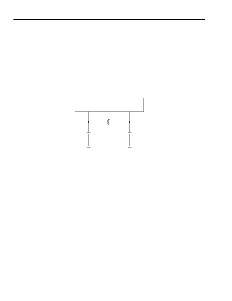
13 Crystal Electrical Characteristics and Requirements
If the option for using the external crystal is chosen, the following electrical characteristics and requirements apply.
13.1 External Components for the Crystal Oscillator
The crystal oscillator is enabled by connecting a crystal across CKI and CKI2, along with one external capacitor from
each of these pins to ground (see Figure 83). For most applications, 10 pF external capacitors are recommended;
however, larger values allow for better frequency precision (see Section 13.4, Frequency Accuracy Considerations).
The crystal should be either fundamental or overtone mode, parallel resonant, with a rated power (drive level) of at
least 1 mW, and specified at a load capacitance equal to the total capacitance seen by the crystal (including external
capacitors and strays). The series resistance of the crystal should be specified to be less than
half
the absolute
value of the negative resistance shown in Figure 84 or Figure 85 for the crystal frequency. The frequency of the
signal at the CKI input pin is equal to the crystal frequency.
Figure 83. Fundamental Crystal Configuration
The following guidelines should be followed when designing the printed-circuit board layout for a crystal-based ap-
plication:
1. Keep crystal and external capacitors as close to CKI and CKI2 pins as possible to minimize board stray capaci-
tance.
2. Keep high-frequency digital signals such as CKO away from CKI and CKI2 traces to avoid coupling.
13.2 Power Dissipation
Figures 86 and 87 indicate the typical power dissipation of the on-chip crystal oscillator circuit versus frequency.
Note that these curves are intended to show the relative effects of load capacitance on supply current and that the
actual supply current measured depends on crystal resistance. For typical crystals, measured supply current at the
V
DDA
pin should be less than that shown in the figures.
5-4041 (F).a
CKI
CKI2
XTAL
C
1
C
2
相關(guān)PDF資料 |
PDF描述 |
|---|---|
| DSP1629 | TVS 400W 64V UNIDIRECT SMA |
| DSP16410C | TVS 400W 7.0V UNIDIRECT SMA |
| DSP16410 | 16-bit fixed point DSP with Flash |
| DSP25-16AR | Phase-leg Rectifier Diode |
| DSP25 | Phase-leg Rectifier Diode |
相關(guān)代理商/技術(shù)參數(shù) |
參數(shù)描述 |
|---|---|
| DSP1627F32K10IR | 制造商:未知廠家 制造商全稱(chēng):未知廠家 功能描述:DSP|16-BIT|CMOS|QFP|100PIN|PLASTIC |
| DSP1627F32K10IT | 制造商:未知廠家 制造商全稱(chēng):未知廠家 功能描述:DSP|16-BIT|CMOS|QFP|100PIN|PLASTIC |
| DSP1627F32K11I | 制造商:未知廠家 制造商全稱(chēng):未知廠家 功能描述:16-Bit Digital Signal Processor |
| DSP1627F32K11IR | 制造商:未知廠家 制造商全稱(chēng):未知廠家 功能描述:DSP|16-BIT|CMOS|QFP|100PIN|PLASTIC |
| DSP1627F32K11IT | 制造商:未知廠家 制造商全稱(chēng):未知廠家 功能描述:DSP|16-BIT|CMOS|QFP|100PIN|PLASTIC |
發(fā)布緊急采購(gòu),3分鐘左右您將得到回復(fù)。