- 您現(xiàn)在的位置:買(mǎi)賣(mài)IC網(wǎng) > PDF目錄378216 > 82559 (INTEL CORP) Fast Ethernet Multifunction PCI/CARD bus controller(快速以太網(wǎng)多功能PCI/CARD 總線控制器) PDF資料下載
參數(shù)資料
| 型號(hào): | 82559 |
| 廠商: | INTEL CORP |
| 元件分類(lèi): | 微控制器/微處理器 |
| 英文描述: | Fast Ethernet Multifunction PCI/CARD bus controller(快速以太網(wǎng)多功能PCI/CARD 總線控制器) |
| 中文描述: | 1 CHANNEL(S), 100M bps, LOCAL AREA NETWORK CONTROLLER, PBGA196 |
| 封裝: | 15 X 15 MM, BGA-196 |
| 文件頁(yè)數(shù): | 20/124頁(yè) |
| 文件大小: | 1332K |
| 代理商: | 82559 |
第1頁(yè)第2頁(yè)第3頁(yè)第4頁(yè)第5頁(yè)第6頁(yè)第7頁(yè)第8頁(yè)第9頁(yè)第10頁(yè)第11頁(yè)第12頁(yè)第13頁(yè)第14頁(yè)第15頁(yè)第16頁(yè)第17頁(yè)第18頁(yè)第19頁(yè)當(dāng)前第20頁(yè)第21頁(yè)第22頁(yè)第23頁(yè)第24頁(yè)第25頁(yè)第26頁(yè)第27頁(yè)第28頁(yè)第29頁(yè)第30頁(yè)第31頁(yè)第32頁(yè)第33頁(yè)第34頁(yè)第35頁(yè)第36頁(yè)第37頁(yè)第38頁(yè)第39頁(yè)第40頁(yè)第41頁(yè)第42頁(yè)第43頁(yè)第44頁(yè)第45頁(yè)第46頁(yè)第47頁(yè)第48頁(yè)第49頁(yè)第50頁(yè)第51頁(yè)第52頁(yè)第53頁(yè)第54頁(yè)第55頁(yè)第56頁(yè)第57頁(yè)第58頁(yè)第59頁(yè)第60頁(yè)第61頁(yè)第62頁(yè)第63頁(yè)第64頁(yè)第65頁(yè)第66頁(yè)第67頁(yè)第68頁(yè)第69頁(yè)第70頁(yè)第71頁(yè)第72頁(yè)第73頁(yè)第74頁(yè)第75頁(yè)第76頁(yè)第77頁(yè)第78頁(yè)第79頁(yè)第80頁(yè)第81頁(yè)第82頁(yè)第83頁(yè)第84頁(yè)第85頁(yè)第86頁(yè)第87頁(yè)第88頁(yè)第89頁(yè)第90頁(yè)第91頁(yè)第92頁(yè)第93頁(yè)第94頁(yè)第95頁(yè)第96頁(yè)第97頁(yè)第98頁(yè)第99頁(yè)第100頁(yè)第101頁(yè)第102頁(yè)第103頁(yè)第104頁(yè)第105頁(yè)第106頁(yè)第107頁(yè)第108頁(yè)第109頁(yè)第110頁(yè)第111頁(yè)第112頁(yè)第113頁(yè)第114頁(yè)第115頁(yè)第116頁(yè)第117頁(yè)第118頁(yè)第119頁(yè)第120頁(yè)第121頁(yè)第122頁(yè)第123頁(yè)第124頁(yè)
82559 — Networking Silicon
10
Datasheet
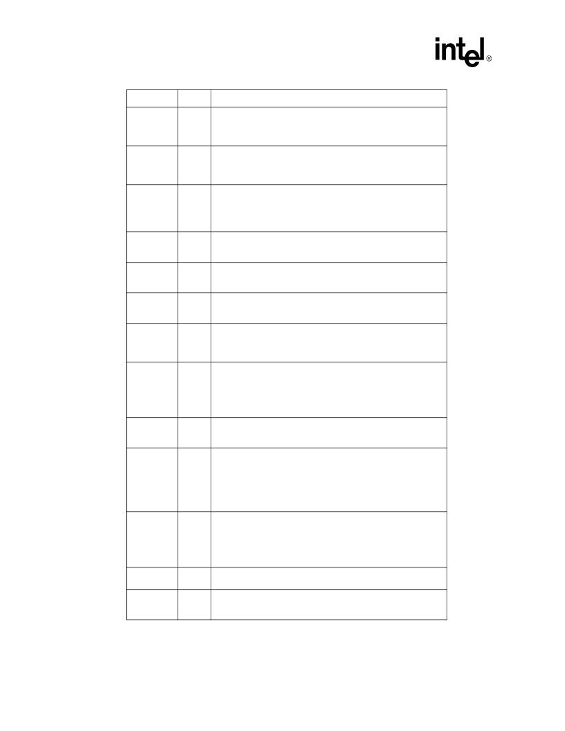
FLA[14]/
EEDO
IN/OUT
Flash Address[14]/EEPROM Data Output.
During Flash accesses,
this multiplexed pin acts as the Flash Address [14] output signal.
During EEPROM accesses, it acts as serial input data to the EEPROM
Data Output signal.
FLA[13]/
EEDI
OUT
Flash Address[13]/EEPROM Data Input.
During Flash accesses,
this multiplexed pin acts as the Flash Address [13] output signal.
During EEPROM accesses, it acts as serial output data to the
EEPROM Data Input signal.
FLA[12]/
MCNTSM#
OUT
O/D
Flash Address[12]/Modem Central Site Mode.
This multiplexed pin
acts as the Flash Address[12] output signal in a non-modem card. If
modem is enabled, it is used as an output signal to the modem. It is
either floated by default or driven low by the Modem System Control
Registers.
FLA[11]/
MINT
IN/OUT
Flash Address[11]/Modem Interrupt.
This multiplexed pin acts as
the Flash Address[11] output signal in a non-modem card. If modem is
enabled, it is used as the Modem Interrupt input signal.
FLA[10]/
MRING#
IN/OUT
Flash Address[10]/Modem Ring.
This multiplexed pin acts as the
Flash Address[10] output signal in a non-modem card. If modem is
enabled, it is used as the Modem Ring input signal.
FLA[9]/
MRST
OUT
Flash Address[9]/Modem Reset.
This multiplexed pin acts as the
Flash Address[9] output signal in a non-modem card. If modem is
enabled, it acts as the Modem Reset signal with an active high output.
FLA[8]/
IOCHRDY
IN/OUT
Flash Address[8]/ISA Input/Output Channel Ready.
This
multiplexed pin acts as the Flash Address[8] output signal in a non-
modem card. If modem is enabled, it is used as the ISA IOCHRDY
input signal.
FLA[7]/
CLKEN
T/S
Flash Address[7]/Clock Enable.
This is a multiplexed pin and acts
as the Flash Address[7] output signal during nominal operation. When
the PCI RST# signal is active, this pin acts as input control over the
FLA[16]/CLK25 output signal. If the FLA[7]/CLKEN pin is connected to
a pull-up resistor (3.3 K
), a 25 MHz clock signal is provided on the
FLA[16]/CLK25 output; otherwise, it is used as FLA[16] output.
FLA[6:2]
OUT
Flash Address[6:2].
These pins are used as Flash address outputs
to support 128 Kbyte Flash addressing. If the modem is enabled,
these pins carry modem address bits 6:2.
FLA[1]/
AUXPWR
T/S
Flash Address[1]/Auxiliary Power.
This multiplexed pin acts as the
Flash Address[1] output signal during nominal operation. If the modem
is enabled, this pin carries modem address bit 1. When RST is active
(low), it acts as the power supply indicator. If the 82559 is fed PCI
power, this pin should be connected to a pull-down resistor; if the
82559 is fed by auxiliary power, this pin should be connected to a pull-
up resistor.
FLA[0]/
PCIMODE#
T/S
Flash Address [0]/PCI Mode.
This multiplexed pin acts as the Flash
Address[0] output signal during nominal operation. If the modem is
enabled, this pin carries modem address bit 0. When RST# is active
(low), it acts as the input system type. If the 82559 is used in a
CardBus system, this pin should be connected to a pull-up resistor
(3.3 K
); otherwise, the 82559 considers the host as a PCI system.
EECS
OUT
EEPROM Chip Select.
The EEPROM Chip Select signal is used to
assert chip select to the serial EEPROM.
FLCS#/AEN
OUT
Flash Chip Select/Address Enable.
The Flash Chip Select signal is
active during Flash. In modem mode, it acts as an ISA-like Address
Enable signal (modem chip select).
Symbol
Type
Name and Function
相關(guān)PDF資料 |
PDF描述 |
|---|---|
| 8255A-5 | PROGRAMMABLE PERIPHEAL INTERFACE |
| 8255A | IC LOGIC 3257 4-BIT 1-OF-2 FET MULTIPLEXER/DEMULTIPLEXER -40+85C SSOP-16 - OBSOLETE |
| 8255A | Programmable Peripheral Interface iAPX86 Family |
| 8255A-5 | 12-Bit, 2.7 V to 5.25 V, 1.5 MSPS Low Power ADC; Package: SOIC - Wide; No of Pins: 24; Temperature Range: Industrial |
| 82562G | Mbps Platform LAN Connect |
相關(guān)代理商/技術(shù)參數(shù) |
參數(shù)描述 |
|---|---|
| 82-5590 | 制造商:Amphenol RF 功能描述:Connector Twinax Receptacle 0Hz to 500MHz Solder Straight Ca |
| 825590-1 | 功能描述:手工工具 HANDTOOL FOR TIMER CONT RoHS:否 制造商:Molex 產(chǎn)品:Extraction Tools 類(lèi)型: 描述/功能:Extraction tool |
| 82-5590-2RFX | 功能描述:RF 連接器 FRONT MNT BH RECEPT RoHS:否 制造商:Bomar Interconnect 產(chǎn)品:Connectors 射頻系列:BNC 型式:Jack (Female) 極性: 觸點(diǎn)電鍍:Gold 阻抗: 端接類(lèi)型:Solder 主體類(lèi)型:Straight Bulkhead 電纜類(lèi)型: |
| 82-5590-RFX | 功能描述:RF 連接器 BULKHEAD JACK S/CUP FRONT MOUNT RoHS:否 制造商:Bomar Interconnect 產(chǎn)品:Connectors 射頻系列:BNC 型式:Jack (Female) 極性: 觸點(diǎn)電鍍:Gold 阻抗: 端接類(lèi)型:Solder 主體類(lèi)型:Straight Bulkhead 電纜類(lèi)型: |
| 825591 | 功能描述:手工工具 D.A. HANDTOOL ASSY RoHS:否 制造商:Molex 產(chǎn)品:Extraction Tools 類(lèi)型: 描述/功能:Extraction tool |
發(fā)布緊急采購(gòu),3分鐘左右您將得到回復(fù)。