- 您現(xiàn)在的位置:買賣IC網(wǎng) > PDF目錄1977 > XRT79L71IB-F (Exar Corporation)IC LIU/FRAMER DS3/E3 1CH 208BGA PDF資料下載
參數(shù)資料
| 型號(hào): | XRT79L71IB-F |
| 廠商: | Exar Corporation |
| 文件頁(yè)數(shù): | 278/609頁(yè) |
| 文件大?。?/td> | 0K |
| 描述: | IC LIU/FRAMER DS3/E3 1CH 208BGA |
| 標(biāo)準(zhǔn)包裝: | 126 |
| 控制器類型: | DS3/E3 調(diào)幀器 |
| 接口: | LIU |
| 電源電壓: | 3.15 V ~ 3.45 V |
| 工作溫度: | -40°C ~ 85°C |
| 安裝類型: | 表面貼裝 |
| 封裝/外殼: | 208-LBGA |
| 供應(yīng)商設(shè)備封裝: | 208-STBGA(17x17) |
| 包裝: | 托盤 |
第1頁(yè)第2頁(yè)第3頁(yè)第4頁(yè)第5頁(yè)第6頁(yè)第7頁(yè)第8頁(yè)第9頁(yè)第10頁(yè)第11頁(yè)第12頁(yè)第13頁(yè)第14頁(yè)第15頁(yè)第16頁(yè)第17頁(yè)第18頁(yè)第19頁(yè)第20頁(yè)第21頁(yè)第22頁(yè)第23頁(yè)第24頁(yè)第25頁(yè)第26頁(yè)第27頁(yè)第28頁(yè)第29頁(yè)第30頁(yè)第31頁(yè)第32頁(yè)第33頁(yè)第34頁(yè)第35頁(yè)第36頁(yè)第37頁(yè)第38頁(yè)第39頁(yè)第40頁(yè)第41頁(yè)第42頁(yè)第43頁(yè)第44頁(yè)第45頁(yè)第46頁(yè)第47頁(yè)第48頁(yè)第49頁(yè)第50頁(yè)第51頁(yè)第52頁(yè)第53頁(yè)第54頁(yè)第55頁(yè)第56頁(yè)第57頁(yè)第58頁(yè)第59頁(yè)第60頁(yè)第61頁(yè)第62頁(yè)第63頁(yè)第64頁(yè)第65頁(yè)第66頁(yè)第67頁(yè)第68頁(yè)第69頁(yè)第70頁(yè)第71頁(yè)第72頁(yè)第73頁(yè)第74頁(yè)第75頁(yè)第76頁(yè)第77頁(yè)第78頁(yè)第79頁(yè)第80頁(yè)第81頁(yè)第82頁(yè)第83頁(yè)第84頁(yè)第85頁(yè)第86頁(yè)第87頁(yè)第88頁(yè)第89頁(yè)第90頁(yè)第91頁(yè)第92頁(yè)第93頁(yè)第94頁(yè)第95頁(yè)第96頁(yè)第97頁(yè)第98頁(yè)第99頁(yè)第100頁(yè)第101頁(yè)第102頁(yè)第103頁(yè)第104頁(yè)第105頁(yè)第106頁(yè)第107頁(yè)第108頁(yè)第109頁(yè)第110頁(yè)第111頁(yè)第112頁(yè)第113頁(yè)第114頁(yè)第115頁(yè)第116頁(yè)第117頁(yè)第118頁(yè)第119頁(yè)第120頁(yè)第121頁(yè)第122頁(yè)第123頁(yè)第124頁(yè)第125頁(yè)第126頁(yè)第127頁(yè)第128頁(yè)第129頁(yè)第130頁(yè)第131頁(yè)第132頁(yè)第133頁(yè)第134頁(yè)第135頁(yè)第136頁(yè)第137頁(yè)第138頁(yè)第139頁(yè)第140頁(yè)第141頁(yè)第142頁(yè)第143頁(yè)第144頁(yè)第145頁(yè)第146頁(yè)第147頁(yè)第148頁(yè)第149頁(yè)第150頁(yè)第151頁(yè)第152頁(yè)第153頁(yè)第154頁(yè)第155頁(yè)第156頁(yè)第157頁(yè)第158頁(yè)第159頁(yè)第160頁(yè)第161頁(yè)第162頁(yè)第163頁(yè)第164頁(yè)第165頁(yè)第166頁(yè)第167頁(yè)第168頁(yè)第169頁(yè)第170頁(yè)第171頁(yè)第172頁(yè)第173頁(yè)第174頁(yè)第175頁(yè)第176頁(yè)第177頁(yè)第178頁(yè)第179頁(yè)第180頁(yè)第181頁(yè)第182頁(yè)第183頁(yè)第184頁(yè)第185頁(yè)第186頁(yè)第187頁(yè)第188頁(yè)第189頁(yè)第190頁(yè)第191頁(yè)第192頁(yè)第193頁(yè)第194頁(yè)第195頁(yè)第196頁(yè)第197頁(yè)第198頁(yè)第199頁(yè)第200頁(yè)第201頁(yè)第202頁(yè)第203頁(yè)第204頁(yè)第205頁(yè)第206頁(yè)第207頁(yè)第208頁(yè)第209頁(yè)第210頁(yè)第211頁(yè)第212頁(yè)第213頁(yè)第214頁(yè)第215頁(yè)第216頁(yè)第217頁(yè)第218頁(yè)第219頁(yè)第220頁(yè)第221頁(yè)第222頁(yè)第223頁(yè)第224頁(yè)第225頁(yè)第226頁(yè)第227頁(yè)第228頁(yè)第229頁(yè)第230頁(yè)第231頁(yè)第232頁(yè)第233頁(yè)第234頁(yè)第235頁(yè)第236頁(yè)第237頁(yè)第238頁(yè)第239頁(yè)第240頁(yè)第241頁(yè)第242頁(yè)第243頁(yè)第244頁(yè)第245頁(yè)第246頁(yè)第247頁(yè)第248頁(yè)第249頁(yè)第250頁(yè)第251頁(yè)第252頁(yè)第253頁(yè)第254頁(yè)第255頁(yè)第256頁(yè)第257頁(yè)第258頁(yè)第259頁(yè)第260頁(yè)第261頁(yè)第262頁(yè)第263頁(yè)第264頁(yè)第265頁(yè)第266頁(yè)第267頁(yè)第268頁(yè)第269頁(yè)第270頁(yè)第271頁(yè)第272頁(yè)第273頁(yè)第274頁(yè)第275頁(yè)第276頁(yè)第277頁(yè)當(dāng)前第278頁(yè)第279頁(yè)第280頁(yè)第281頁(yè)第282頁(yè)第283頁(yè)第284頁(yè)第285頁(yè)第286頁(yè)第287頁(yè)第288頁(yè)第289頁(yè)第290頁(yè)第291頁(yè)第292頁(yè)第293頁(yè)第294頁(yè)第295頁(yè)第296頁(yè)第297頁(yè)第298頁(yè)第299頁(yè)第300頁(yè)第301頁(yè)第302頁(yè)第303頁(yè)第304頁(yè)第305頁(yè)第306頁(yè)第307頁(yè)第308頁(yè)第309頁(yè)第310頁(yè)第311頁(yè)第312頁(yè)第313頁(yè)第314頁(yè)第315頁(yè)第316頁(yè)第317頁(yè)第318頁(yè)第319頁(yè)第320頁(yè)第321頁(yè)第322頁(yè)第323頁(yè)第324頁(yè)第325頁(yè)第326頁(yè)第327頁(yè)第328頁(yè)第329頁(yè)第330頁(yè)第331頁(yè)第332頁(yè)第333頁(yè)第334頁(yè)第335頁(yè)第336頁(yè)第337頁(yè)第338頁(yè)第339頁(yè)第340頁(yè)第341頁(yè)第342頁(yè)第343頁(yè)第344頁(yè)第345頁(yè)第346頁(yè)第347頁(yè)第348頁(yè)第349頁(yè)第350頁(yè)第351頁(yè)第352頁(yè)第353頁(yè)第354頁(yè)第355頁(yè)第356頁(yè)第357頁(yè)第358頁(yè)第359頁(yè)第360頁(yè)第361頁(yè)第362頁(yè)第363頁(yè)第364頁(yè)第365頁(yè)第366頁(yè)第367頁(yè)第368頁(yè)第369頁(yè)第370頁(yè)第371頁(yè)第372頁(yè)第373頁(yè)第374頁(yè)第375頁(yè)第376頁(yè)第377頁(yè)第378頁(yè)第379頁(yè)第380頁(yè)第381頁(yè)第382頁(yè)第383頁(yè)第384頁(yè)第385頁(yè)第386頁(yè)第387頁(yè)第388頁(yè)第389頁(yè)第390頁(yè)第391頁(yè)第392頁(yè)第393頁(yè)第394頁(yè)第395頁(yè)第396頁(yè)第397頁(yè)第398頁(yè)第399頁(yè)第400頁(yè)第401頁(yè)第402頁(yè)第403頁(yè)第404頁(yè)第405頁(yè)第406頁(yè)第407頁(yè)第408頁(yè)第409頁(yè)第410頁(yè)第411頁(yè)第412頁(yè)第413頁(yè)第414頁(yè)第415頁(yè)第416頁(yè)第417頁(yè)第418頁(yè)第419頁(yè)第420頁(yè)第421頁(yè)第422頁(yè)第423頁(yè)第424頁(yè)第425頁(yè)第426頁(yè)第427頁(yè)第428頁(yè)第429頁(yè)第430頁(yè)第431頁(yè)第432頁(yè)第433頁(yè)第434頁(yè)第435頁(yè)第436頁(yè)第437頁(yè)第438頁(yè)第439頁(yè)第440頁(yè)第441頁(yè)第442頁(yè)第443頁(yè)第444頁(yè)第445頁(yè)第446頁(yè)第447頁(yè)第448頁(yè)第449頁(yè)第450頁(yè)第451頁(yè)第452頁(yè)第453頁(yè)第454頁(yè)第455頁(yè)第456頁(yè)第457頁(yè)第458頁(yè)第459頁(yè)第460頁(yè)第461頁(yè)第462頁(yè)第463頁(yè)第464頁(yè)第465頁(yè)第466頁(yè)第467頁(yè)第468頁(yè)第469頁(yè)第470頁(yè)第471頁(yè)第472頁(yè)第473頁(yè)第474頁(yè)第475頁(yè)第476頁(yè)第477頁(yè)第478頁(yè)第479頁(yè)第480頁(yè)第481頁(yè)第482頁(yè)第483頁(yè)第484頁(yè)第485頁(yè)第486頁(yè)第487頁(yè)第488頁(yè)第489頁(yè)第490頁(yè)第491頁(yè)第492頁(yè)第493頁(yè)第494頁(yè)第495頁(yè)第496頁(yè)第497頁(yè)第498頁(yè)第499頁(yè)第500頁(yè)第501頁(yè)第502頁(yè)第503頁(yè)第504頁(yè)第505頁(yè)第506頁(yè)第507頁(yè)第508頁(yè)第509頁(yè)第510頁(yè)第511頁(yè)第512頁(yè)第513頁(yè)第514頁(yè)第515頁(yè)第516頁(yè)第517頁(yè)第518頁(yè)第519頁(yè)第520頁(yè)第521頁(yè)第522頁(yè)第523頁(yè)第524頁(yè)第525頁(yè)第526頁(yè)第527頁(yè)第528頁(yè)第529頁(yè)第530頁(yè)第531頁(yè)第532頁(yè)第533頁(yè)第534頁(yè)第535頁(yè)第536頁(yè)第537頁(yè)第538頁(yè)第539頁(yè)第540頁(yè)第541頁(yè)第542頁(yè)第543頁(yè)第544頁(yè)第545頁(yè)第546頁(yè)第547頁(yè)第548頁(yè)第549頁(yè)第550頁(yè)第551頁(yè)第552頁(yè)第553頁(yè)第554頁(yè)第555頁(yè)第556頁(yè)第557頁(yè)第558頁(yè)第559頁(yè)第560頁(yè)第561頁(yè)第562頁(yè)第563頁(yè)第564頁(yè)第565頁(yè)第566頁(yè)第567頁(yè)第568頁(yè)第569頁(yè)第570頁(yè)第571頁(yè)第572頁(yè)第573頁(yè)第574頁(yè)第575頁(yè)第576頁(yè)第577頁(yè)第578頁(yè)第579頁(yè)第580頁(yè)第581頁(yè)第582頁(yè)第583頁(yè)第584頁(yè)第585頁(yè)第586頁(yè)第587頁(yè)第588頁(yè)第589頁(yè)第590頁(yè)第591頁(yè)第592頁(yè)第593頁(yè)第594頁(yè)第595頁(yè)第596頁(yè)第597頁(yè)第598頁(yè)第599頁(yè)第600頁(yè)第601頁(yè)第602頁(yè)第603頁(yè)第604頁(yè)第605頁(yè)第606頁(yè)第607頁(yè)第608頁(yè)第609頁(yè)
PRELIMINARY
XRT79L71
334
REV. P2.0.0
1-CHANNEL DS3/E3 CLEAR-CHANNEL FRAMERLIU COMBO - CC/HDLC ARCHITECTURE
Each of these requirements, and how the XRT79L71 performs against these requirements is described in
detail below.
5.2.5.2.1
The Basic Architecture of the Jitter Attenuator Block
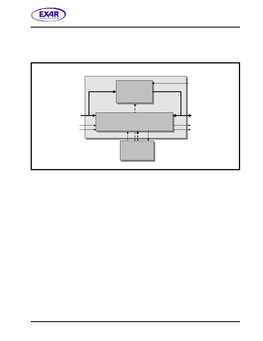
According to Figure 154, the Jitter Attenuator consists of the following functional blocks.
The Timing Control/Phase-Locked Loop Block
The Jitter Attenuator FIFO
How the Jitter Attenuator Works
The Jitter Attenuator Block (within the XRT79L71) will accept "jittery" clock (In_Clk) and data signals (In_POS
and In_NEG) from either the HDB3/B3ZS Encoder Block (if the Jitter Attenuator has been configured to
operate in the Transmit Direction) or from the "Clock and Data Recovery" Block (if the Jitter Attenuator has
been configured to operate in the Receive Direction). The Jitter Attenuator block will latch the data, residing on
internal signals "In_POS" and "In_NEG" into the "Jitter Attenuator FIFO" upon the appropriate edge of the
In_Clk signal.
In parallel, the In_Clk signal will also be routed to the "Timing Control/PLL" Block. This block consists of a
Narrow-band PLL which has the responsibility of attenuating much of the jitter within the "In_Clk" signal. The
"smoothed" version of this clock signal will be output from the Jitter Attenuator block (and is designated as
"Out_Clk" in Figure 154). Further, the "Jittery Data" (which was latched into the Jitter Attenuator FIFO via the
"In_Clk" signal) will now be clocked out of the Jitter Attenuator block via the "Out_Clk" signal.
NOTES:
1.
If the Jitter Attenuator block has been configured to operate in the "Transmit Direction" and if the XRT79L71 has
been configured to operate in the "Local-Timing" Mode, then the "In_CLK" signal (as depicted in
above) will be a buffered version of clock signal being applied to the "TxInClk" input pin.
2.
If the Jitter Attenuator block has been configured to operate in the Transmit Direction" and if the XRT79L71 has
been configured to operate in the "Loop-Timing" Mode, then the "In_CLK" signal (as depicted in F
above) will be a buffered version of the "Recovered" clock signal (from the Receive DS3/E3 LIU Block).
FIGURE 154. AN ILLUSTRATION OF THE FUNCTIONAL BLOCK DIAGRAM OF THE JITTER ATTENUATOR BLOCK
Timing Control
Block/
Phase Locked
Loop
Timing Control
Block/
Phase Locked
Loop
In_POS
In_NEG
In_CLK
Write_Clock
Read_Clock
Out_POS
Out_NEG
Out_CLK
Microprocessor
Interface
16/32 Bit FIFO
Jittery Clock
Smoothed Clock
FL
DS3Clk/E3Clk
Or SFM-Derived
Line Code
JA_RESET
相關(guān)PDF資料 |
PDF描述 |
|---|---|
| XRT81L27IV-F | IC LIU EI 7CH 3.3V 128TQFP |
| XRT82D20IW-F | IC LIU E1 SGL 28SOJ |
| XRT82L24AIV-F | IC LIU E1 QAUD 100TQFP |
| XRT83D10IW | IC LIU T1/E1 SGL 28SOJ |
| XRT83L30IV-F | IC LIU LH/SH T1/E1 SGL 64TQFP |
相關(guān)代理商/技術(shù)參數(shù) |
參數(shù)描述 |
|---|---|
| XRT79L72 | 制造商:EXAR 制造商全稱:EXAR 功能描述:2 - CHANNEL DS3/E3 ATM UNI/PPP COMBO IC |
| XRT79L72IB | 制造商:EXAR 制造商全稱:EXAR 功能描述:2 - CHANNEL DS3/E3 ATM UNI/PPP COMBO IC |
| XRT79L73 | 制造商:EXAR 制造商全稱:EXAR 功能描述:3 - CHANNEL DS3/E3 ATM UNI/PPP COMBO IC |
| XRT79L73IB | 制造商:EXAR 制造商全稱:EXAR 功能描述:3 - CHANNEL DS3/E3 ATM UNI/PPP COMBO IC |
| XRT79L74 | 制造商:EXAR 制造商全稱:EXAR 功能描述:4 - CHANNEL DS3/E3 ATM UNI/PPP COMBO IC |
發(fā)布緊急采購(gòu),3分鐘左右您將得到回復(fù)。