- 您現(xiàn)在的位置:買賣IC網(wǎng) > PDF目錄361591 > uPSD3233 (意法半導(dǎo)體) Flash Programmable System Device with 8032 Microcontroller Core(嵌入高速“8032微控制器核”的Flash型可編程系統(tǒng)器) PDF資料下載
參數(shù)資料
| 型號: | uPSD3233 |
| 廠商: | 意法半導(dǎo)體 |
| 英文描述: | Flash Programmable System Device with 8032 Microcontroller Core(嵌入高速“8032微控制器核”的Flash型可編程系統(tǒng)器) |
| 中文描述: | 閃存可編程系統(tǒng)器件與8032微控制器內(nèi)核(嵌入高速“8032微控制器核”的閃存型可編程系統(tǒng)器) |
| 文件頁數(shù): | 131/164頁 |
| 文件大小: | 1133K |
| 代理商: | UPSD3233 |
第1頁第2頁第3頁第4頁第5頁第6頁第7頁第8頁第9頁第10頁第11頁第12頁第13頁第14頁第15頁第16頁第17頁第18頁第19頁第20頁第21頁第22頁第23頁第24頁第25頁第26頁第27頁第28頁第29頁第30頁第31頁第32頁第33頁第34頁第35頁第36頁第37頁第38頁第39頁第40頁第41頁第42頁第43頁第44頁第45頁第46頁第47頁第48頁第49頁第50頁第51頁第52頁第53頁第54頁第55頁第56頁第57頁第58頁第59頁第60頁第61頁第62頁第63頁第64頁第65頁第66頁第67頁第68頁第69頁第70頁第71頁第72頁第73頁第74頁第75頁第76頁第77頁第78頁第79頁第80頁第81頁第82頁第83頁第84頁第85頁第86頁第87頁第88頁第89頁第90頁第91頁第92頁第93頁第94頁第95頁第96頁第97頁第98頁第99頁第100頁第101頁第102頁第103頁第104頁第105頁第106頁第107頁第108頁第109頁第110頁第111頁第112頁第113頁第114頁第115頁第116頁第117頁第118頁第119頁第120頁第121頁第122頁第123頁第124頁第125頁第126頁第127頁第128頁第129頁第130頁當(dāng)前第131頁第132頁第133頁第134頁第135頁第136頁第137頁第138頁第139頁第140頁第141頁第142頁第143頁第144頁第145頁第146頁第147頁第148頁第149頁第150頁第151頁第152頁第153頁第154頁第155頁第156頁第157頁第158頁第159頁第160頁第161頁第162頁第163頁第164頁
131/164
μ
PSD3200 FAMILY
DRAFT(Thursday 20 June 2002, 13:15).
PROGRAMMING IN-CIRCUIT USING THE JTAG SERIAL INTERFACE
The JTAG Serial Interface block can be enabled
on Port C(see Table104). Allmemory blocks (pri-
mary and secondary Flash memory), PLD logic,
and PSD Module Configuration Register bits may
be programmedthrough the JTAG Serial Interface
block. A blank device can be mounted on a printed
circuit board and programmed using JTAG.
The standard JTAG signals (IEEE 1149.1) are
TMS, TCK, TDI, and TDO. Twoadditional signals,
TSTAT and TERR, are optional JTAG extensions
used to speed up Program and Erase cycles.
By default, on a blank PSD Module (as shipped
from thefactory or after erasure), four pins on Port
C are enabled for the basic JTAG signals TMS,
TCK, TDI, and TDO
See Application Note AN1153 for more details on
JTAG In-System Programming (ISP).
Standard JTAG Signals
The standard JTAG signals (TMS, TCK, TDI, and
TDO) canbe enabled by any of three different con-
ditions that are logically ORed. When enabled,
TDI, TDO, TCK, and TMS are inputs, waiting for a
JTAG serial command froman external JTAGcon-
troller device (such as FlashLINK or Automated
Test Equipment). When the enabling command is
received, TDO becomes an output and the JTAG
channel is fully functional. The same command
that enables the JTAG channel mayoptionally en-
able the two additional JTAG signals, TSTAT and
TERR.
The following symbolic logic equationspecifies the
conditions enabling the four basic JTAG signals
(TMS, TCK, TDI, and TDO) on their respective
Port C pins. For purposes of discussion, the logic
label JTAG_ON is used. When JTAG_ON is true,
the four pins are enabled for JTAG. When
JTAG_ON is false, the four pins can be used for
general PSD Module I/O.
JTAG_ON = PSDsoft_enabled +
/* An NVM configuration bit inside the
PSD Module is set by the designer in
the
PSDsoft
Express
Configuration
utility. This dedicates
the pins for
JTAG at all times (compliant with IEEE
1149.1 */
8032_Module_enabled +
/* The MCU can set a bit at run-time by
writing
to
the
PSD
register,
Enable.
This
register
is
address CSIOP + offset C7h. Setting the
JTAG_ENABLE bit in this register will
enable the pins for JTAG use. This bit
is cleared by a PSD reset or the MCU.
See Table 105 for bit definition. */
PSD_product_term_enabled;
/* A dedicated product term (PT) inside
the PSD Module can be used to enable
the JTAG pins. This PT has the reserved
name JTAGSEL. Once defined as a node in
PSDsoft,
the
designer
can
JTAG
located
at
write
an
equation
used
multiplexed with other I/O signals. It
is
recommended
to
node JTAGSEL to the JEN\ signal on the
Flashlink cable when multiplexing JTAG
signals. See Application Note 1153 for
details. */
The state of the Reset(RESET) signaldoes notin-
terrupt (or prevent) JTAG operations if the JTAG
pins are dedicated by an NVM configuration bit
(via PSDsoft Express). However, Reset (RESET)
will prevent or interrupt JTAG operations if the
JTAG enable register is used to enable the JTAG
pins.
The
μ
PSD3200 Family supportsJTAG In-System-
Configuration (ISC) commands, but not Boundary
Scan. The PSDsoft Express software tool and
FlashLINK JTAG programming cable implement
the JTAG In-System-Configuration (ISC) com-
mands. A definition of these JTAG In-System-
Configuration (ISC) commands and sequences is
defined in a supplemental document available
from ST. Thisdocument isneeded only as a refer-
ence for designers who use a FlashLINK to pro-
gram the
μ
PSD3200 Family.
for JTAGSEL.
when
the
This method is
JTAG
pins
Port
C
are
logically
tie
the
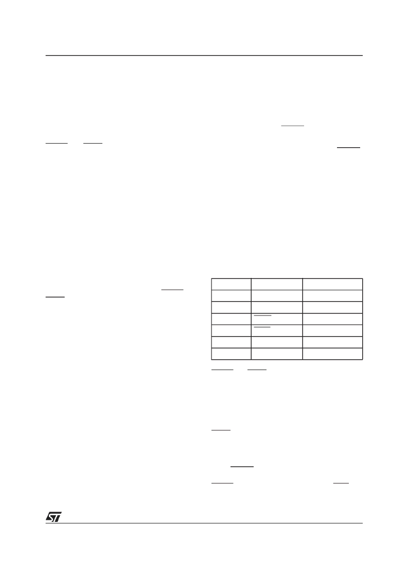
Table 104. JTAG Port Signals
JTAG Extensions
TSTAT and TERR aretwoJTAG extension signals
enabled by an “ISC_ENABLE” command received
over the four standard JTAG signals (TMS, TCK,
TDI, and TDO). They are used to speed Program
and Erase cycles by indicating status on
μ
PDS
signals instead of having to scan the status out se-
rially using the standard JTAG channel. See Appli-
cation Note AN1153
TERR indicates if an error has occurred when
erasing a sector or programming a byte in Flash
memory. This signal goes Low (active) when an
Error condition occurs, and stays Low until an
“ISC_CLEAR” command is executed or a chip Re-
set
(RESET)
pulse
“ISC_DISABLE” command.
TSTAT behaves the same as Ready/Busy de-
scribed inthe section entitled“Ready/Busy (PC3)”,
is
received
after
an
Port C Pin
JTAG Signals
Description
PC0
TMS
Mode Select
PC1
TCK
Clock
PC3
TSTAT
Status
PC4
TERR
Error Flag
PC5
TDI
Serial Data In
PC6
TDO
Serial Data Out
相關(guān)PDF資料 |
PDF描述 |
|---|---|
| uPSD3234(中文) | Flash Programmable System Device with 8032 Microcontroller Core(嵌入高速“8032微控制器核”的Flash型可編程系統(tǒng)器) |
| uPSD3212C(中文) | Flash Programmable System Devices with 8032 Microcontroller Core and 16Kbit SRAM(帶8032微控制器內(nèi)核和16Kbit SRAM的FLASH可編程系統(tǒng)器件) |
| uPSD3254A(中文) | Flash Programmable System Devices with 8032 Microcontroller Core(帶8032微控制器內(nèi)核的FLASH可編程系統(tǒng)器件) |
| uPSD3254BV(中文) | Flash Programmable System Devices with 8032 Microcontroller Core(帶8032微控制器內(nèi)核的FLASH可編程系統(tǒng)器件) |
| UPSD3234A | Flash Programmable System Devices with 8032 Microcontroller Core |
相關(guān)代理商/技術(shù)參數(shù) |
參數(shù)描述 |
|---|---|
| UPSD3233A-24T1 | 制造商:STMICROELECTRONICS 制造商全稱:STMicroelectronics 功能描述:Flash Programmable System Device with 8032 Microcontroller Core |
| UPSD3233A-24T1T | 制造商:STMICROELECTRONICS 制造商全稱:STMicroelectronics 功能描述:Flash Programmable System Devices with 8032 Microcontroller Core |
| UPSD3233A-24T6 | 制造商:STMICROELECTRONICS 制造商全稱:STMicroelectronics 功能描述:Flash Programmable System Device with 8032 Microcontroller Core |
| UPSD3233A-24T6T | 制造商:STMICROELECTRONICS 制造商全稱:STMicroelectronics 功能描述:Flash Programmable System Devices with 8032 Microcontroller Core |
| UPSD3233A-24U1 | 制造商:STMICROELECTRONICS 制造商全稱:STMicroelectronics 功能描述:Flash Programmable System Device with 8032 Microcontroller Core |
發(fā)布緊急采購,3分鐘左右您將得到回復(fù)。