- 您現(xiàn)在的位置:買賣IC網(wǎng) > PDF目錄368064 > PM5372-BI Telecommunication IC PDF資料下載
參數(shù)資料
| 型號: | PM5372-BI |
| 英文描述: | Telecommunication IC |
| 中文描述: | 通信集成電路 |
| 文件頁數(shù): | 149/169頁 |
| 文件大?。?/td> | 989K |
| 代理商: | PM5372-BI |
第1頁第2頁第3頁第4頁第5頁第6頁第7頁第8頁第9頁第10頁第11頁第12頁第13頁第14頁第15頁第16頁第17頁第18頁第19頁第20頁第21頁第22頁第23頁第24頁第25頁第26頁第27頁第28頁第29頁第30頁第31頁第32頁第33頁第34頁第35頁第36頁第37頁第38頁第39頁第40頁第41頁第42頁第43頁第44頁第45頁第46頁第47頁第48頁第49頁第50頁第51頁第52頁第53頁第54頁第55頁第56頁第57頁第58頁第59頁第60頁第61頁第62頁第63頁第64頁第65頁第66頁第67頁第68頁第69頁第70頁第71頁第72頁第73頁第74頁第75頁第76頁第77頁第78頁第79頁第80頁第81頁第82頁第83頁第84頁第85頁第86頁第87頁第88頁第89頁第90頁第91頁第92頁第93頁第94頁第95頁第96頁第97頁第98頁第99頁第100頁第101頁第102頁第103頁第104頁第105頁第106頁第107頁第108頁第109頁第110頁第111頁第112頁第113頁第114頁第115頁第116頁第117頁第118頁第119頁第120頁第121頁第122頁第123頁第124頁第125頁第126頁第127頁第128頁第129頁第130頁第131頁第132頁第133頁第134頁第135頁第136頁第137頁第138頁第139頁第140頁第141頁第142頁第143頁第144頁第145頁第146頁第147頁第148頁當(dāng)前第149頁第150頁第151頁第152頁第153頁第154頁第155頁第156頁第157頁第158頁第159頁第160頁第161頁第162頁第163頁第164頁第165頁第166頁第167頁第168頁第169頁
TSE Transmission Switch Element Datasheet
Released
Proprietary and Confidential to PMC-Sierra, Inc., and for its Customers’ Internal Use
Document ID: PMC-1991258, Issue 7
149
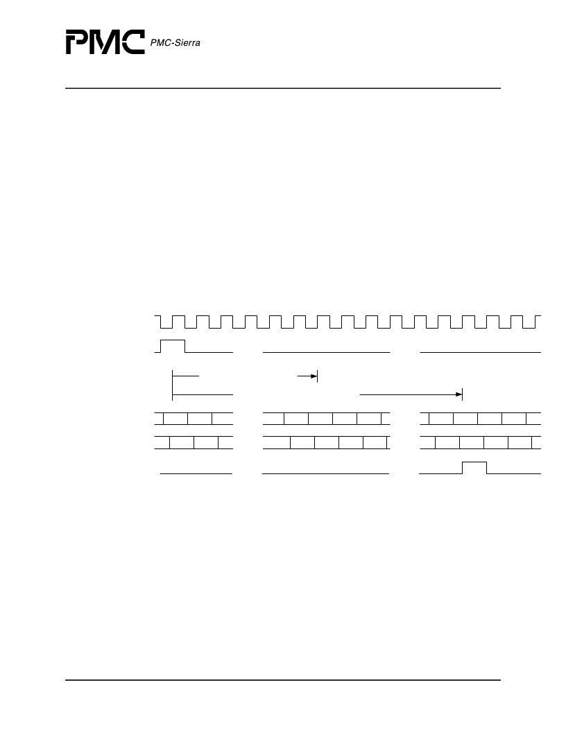
13.2 Transmit Interface Timing
Figure 21 below shows the delay from assertion of RJ0FP to the transmit serial data links. Due to
the presence of FIFOs in the data path, the delay to the various links can differ by up to 8 cycles.
The minimum delay (RJ0DLY + 40 SYSCLK cycles) is shown to be incurred by one of the
transmit serial data links (TP[
X
]/TN[
X
]). The maximum delay (RJ0DLY + 47 cycles) is shown to
be incurred by another transmit serial data links (TP[
Y
]/TN[
Y
]). The suggested setting for
TJ0DLY results in a TJ0FP pulse at the time at which all the transmit serial links have transmitted
their respective J0 characters. The maximum delay from RJ0FP to the transmission of a J0 pulse
is RJ0DLY + 47 cycles. Therefore the suggested setting for TJ0DLY is RJ0DLY+ 47. The relative
phases of the links in Figure 21 are shown for illustrative purposes only. Links may have
different delays than what is shown.
Figure 21 Transmit Interface Timing
TP[
X
]/
TN[
X
]
TN[
Y
]/
TP[
Y
]
...
SYSCLK
RJ0FP
S4,3/
A2
S1,1/J0
S2,1/
Z0
S4,3/
A2
S1,1/J0
S2,1/
Z0
RJ0DLY+ Max Delay(47 cycles) to Last
J0
...
...
RJ0DLY + Min Delay(39
cycles) to First J0
...
...
...
...
TJ0FP
...
Figure 22 below shows the delay from CMP to the transmit serial data links. CMP is valid only at
the RJ0FP pulse time, whether RJ0FP is pulsed or not. It is ignored at other locations in the
transport frame. A change in value to the connection memory page signal (CMP) results in
changing the active switch settings. Given that CMP is sampled on the RJ0FP pulse time 0, the
first data that is switched according to the newly selected connection memory page are the A1
bytes of the second frame following the first J0 byte transmitted by the TSE after offset RJ0DLY
+ 40 cycles. In more absolute terms, the first A1s transmitted by the TSE between offset RJ0DLY
+ 40 + 19416 cycles and RJ0DLY + 47 + 19416 cycles, represent the first data switched
according the connection memory page selected by CMP at the RJ0FP pulse time 0.
相關(guān)PDF資料 |
PDF描述 |
|---|---|
| PM5380 | PMC-2010299 S/UNI-8x155 Telecom Standard Product Data Sheet [1.91 MB] |
| PM554 | Programmable Quad Supply Monitor with Adjustable Reset and Watchdog Timers; Package: SSOP; No of Pins: 16; Temperature Range: -40°C to +85°C |
| PM555 | 1 to 10 watt encapsulated power modules |
| PM556 | Precision Quad Supply Monitor in 6-Lead SOT-23; Package: SOT; No of Pins: 6; Temperature Range: 0°C to +70°C |
| PM560 | Precision Quad Supply Monitor in 6-Lead SOT-23; Package: SOT; No of Pins: 6; Temperature Range: 0°C to +70°C |
相關(guān)代理商/技術(shù)參數(shù) |
參數(shù)描述 |
|---|---|
| PM5372BIP | 制造商:PMC-Sierra 功能描述: |
| PM5372-BI-P | 制造商:PMC-Sierra 功能描述: |
| PM5376HFI | 制造商:PMC-Sierra 功能描述: |
| PM5377 | 制造商:PMC 制造商全稱:PMC 功能描述:Single Chip 96-Port STS-1/STM-0 Cross-Connect |
| PM537CE | 制造商:ARTESYN 制造商全稱:Artesyn Technologies 功能描述:Single, dual and triple output 1 to 10.5 Watt AC/DC encapsulated modules |
發(fā)布緊急采購,3分鐘左右您將得到回復(fù)。