- 您現(xiàn)在的位置:買賣IC網(wǎng) > PDF目錄69029 > MC916X1CTH16B1 (FREESCALE SEMICONDUCTOR INC) 16-BIT, FLASH, 16.78 MHz, MICROCONTROLLER, PQFP120 PDF資料下載
參數(shù)資料
| 型號: | MC916X1CTH16B1 |
| 廠商: | FREESCALE SEMICONDUCTOR INC |
| 元件分類: | 微控制器/微處理器 |
| 英文描述: | 16-BIT, FLASH, 16.78 MHz, MICROCONTROLLER, PQFP120 |
| 封裝: | QFP-120 |
| 文件頁數(shù): | 49/172頁 |
| 文件大小: | 1200K |
| 代理商: | MC916X1CTH16B1 |
第1頁第2頁第3頁第4頁第5頁第6頁第7頁第8頁第9頁第10頁第11頁第12頁第13頁第14頁第15頁第16頁第17頁第18頁第19頁第20頁第21頁第22頁第23頁第24頁第25頁第26頁第27頁第28頁第29頁第30頁第31頁第32頁第33頁第34頁第35頁第36頁第37頁第38頁第39頁第40頁第41頁第42頁第43頁第44頁第45頁第46頁第47頁第48頁當(dāng)前第49頁第50頁第51頁第52頁第53頁第54頁第55頁第56頁第57頁第58頁第59頁第60頁第61頁第62頁第63頁第64頁第65頁第66頁第67頁第68頁第69頁第70頁第71頁第72頁第73頁第74頁第75頁第76頁第77頁第78頁第79頁第80頁第81頁第82頁第83頁第84頁第85頁第86頁第87頁第88頁第89頁第90頁第91頁第92頁第93頁第94頁第95頁第96頁第97頁第98頁第99頁第100頁第101頁第102頁第103頁第104頁第105頁第106頁第107頁第108頁第109頁第110頁第111頁第112頁第113頁第114頁第115頁第116頁第117頁第118頁第119頁第120頁第121頁第122頁第123頁第124頁第125頁第126頁第127頁第128頁第129頁第130頁第131頁第132頁第133頁第134頁第135頁第136頁第137頁第138頁第139頁第140頁第141頁第142頁第143頁第144頁第145頁第146頁第147頁第148頁第149頁第150頁第151頁第152頁第153頁第154頁第155頁第156頁第157頁第158頁第159頁第160頁第161頁第162頁第163頁第164頁第165頁第166頁第167頁第168頁第169頁第170頁第171頁第172頁
MOTOROLA
MC68HC916X1
142
MC68HC916X1TS/D
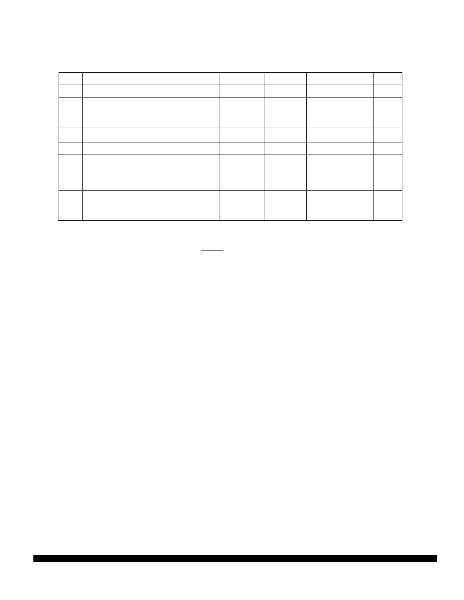
1. Tested with a 4.194 MHz reference.
2. All internal registers retain data at 0 Hz.
3. Assumes that stable VDDSYN is applied, and that the crystal oscillator is stable. Lock time is measured from
the time VDD and VDDSYN are valid until RESET is released. This specification also applies to the period re-
quired for PLL lock after changing the W and Y frequency control bits in the synthesizer control register (SYN-
CR) while the PLL is running, and to the period required for the clock to lock after LPSTOP.
4. This parameter is periodically sampled rather than 100% tested.
5. Assumes that a low-leakage external filter network is used to condition clock synthesizer input voltage. Total
external resistance from the XFC pin due to external leakage must be greater than 15 M
to guarantee this
specification. Filter network geometry can vary depending upon operating environment.
6. Proper layout procedures must be followed to achieve specifications.
7. Internal VCO frequency (fVCO ) is determined by SYNCR W and Y bit values.
The SYNCR X bit controls a divide-by-two circuit that is not in the synthesizer feedback loop.
When X = 0, the divider is enabled, and fsys = fVCO ÷ 4.
When X = 1, the divider is disabled, and fsys = fVCO ÷ 2.
X must equal one when operating at maximum specified fsys.
8. Jitter is the average deviation from the programmed frequency measured over the specified interval at max-
imum fsys. Measurements are made with the device powered by filtered supplies and clocked by a stable ex-
ternal clock signal. Noise injected into the PLL circuitry via VDDSYN and VSS and variation in crystal oscillator
frequency increase the Jclk percentage for a given interval. When clock jitter is a critical constraint on control
system operation, this parameter should be measured during functional testing of the final system.
Table 76 Clock Control Timing
(V
DD
and V
DDSYN
= 5.0 Vdc
± 10 %, V
SS
= 0 Vdc, T
A
= T
L
to T
H
)
Num
Characteristic
Symbol
Min
Max
Unit
1
PLL Reference Frequency Range1
f
ref
3.2
4.2
MHz
2
System Frequency2
On-Chip PLL System Frequency Range
External Clock Operation
f
sys
dc
4(fref) /128
dc
16.78
MHz
3
PLL Lock Time1, 3, 4, 5, 6
t
lpll
—
20
ms
4
VCO Frequency7
fVCO
—
2 (fsys max)
MHz
5
Limp Mode Clock Frequency
SYNCR X bit = 0
SYNCR X bit = 1
f
limp
—
f
sys
max/2
f
sys
max
MHz
6
CLKOUT Jitter1, 4, 5, 6, 8
Short term (5
s interval)
Long term (500
s interval)
J
clk
– 0.5
– 0.05
0.5
0.05
%
F
re
e
sc
a
le
S
e
m
ic
o
n
d
u
c
to
r,
I
Freescale Semiconductor, Inc.
For More Information On This Product,
Go to: www.freescale.com
n
c
..
.
相關(guān)PDF資料 |
PDF描述 |
|---|---|
| SPMC916X1CTH16 | 16-BIT, FLASH, 16.78 MHz, MICROCONTROLLER, PQFP120 |
| MC68HCL05J1ADWR2 | 8-BIT, MROM, 2.1 MHz, MICROCONTROLLER, PDSO20 |
| MC68HC05J1AVDWR2 | 8-BIT, MROM, 2.1 MHz, MICROCONTROLLER, PDSO20 |
| MC68HCP11A1CFNE3 | 8-BIT, EEPROM, 3 MHz, MICROCONTROLLER, PQCC52 |
| MC68HLC705KJ1C | 8-BIT, OTPROM, 4 MHz, MICROCONTROLLER, PDIP16 |
相關(guān)代理商/技術(shù)參數(shù) |
參數(shù)描述 |
|---|---|
| MC92052 | 制造商:MOTOROLA 制造商全稱:Motorola, Inc 功能描述:FTTC User Framer |
| MC92053 | 制造商:MOTOROLA 制造商全稱:Motorola, Inc 功能描述:Quad FTTC Network Framer |
| MC92101CO | 制造商:Rochester Electronics LLC 功能描述:- Bulk |
| MC921G | 制造商:Rochester Electronics LLC 功能描述:- Bulk |
| MC92300 | 制造商:MOTOROLA 制造商全稱:Motorola, Inc 功能描述:VITERBI Decoder for Digital TV |
發(fā)布緊急采購,3分鐘左右您將得到回復(fù)。