- 您現(xiàn)在的位置:買賣IC網(wǎng) > PDF目錄69029 > MC916X1CTH16B1 (FREESCALE SEMICONDUCTOR INC) 16-BIT, FLASH, 16.78 MHz, MICROCONTROLLER, PQFP120 PDF資料下載
參數(shù)資料
| 型號: | MC916X1CTH16B1 |
| 廠商: | FREESCALE SEMICONDUCTOR INC |
| 元件分類: | 微控制器/微處理器 |
| 英文描述: | 16-BIT, FLASH, 16.78 MHz, MICROCONTROLLER, PQFP120 |
| 封裝: | QFP-120 |
| 文件頁數(shù): | 32/172頁 |
| 文件大?。?/td> | 1200K |
| 代理商: | MC916X1CTH16B1 |
第1頁第2頁第3頁第4頁第5頁第6頁第7頁第8頁第9頁第10頁第11頁第12頁第13頁第14頁第15頁第16頁第17頁第18頁第19頁第20頁第21頁第22頁第23頁第24頁第25頁第26頁第27頁第28頁第29頁第30頁第31頁當前第32頁第33頁第34頁第35頁第36頁第37頁第38頁第39頁第40頁第41頁第42頁第43頁第44頁第45頁第46頁第47頁第48頁第49頁第50頁第51頁第52頁第53頁第54頁第55頁第56頁第57頁第58頁第59頁第60頁第61頁第62頁第63頁第64頁第65頁第66頁第67頁第68頁第69頁第70頁第71頁第72頁第73頁第74頁第75頁第76頁第77頁第78頁第79頁第80頁第81頁第82頁第83頁第84頁第85頁第86頁第87頁第88頁第89頁第90頁第91頁第92頁第93頁第94頁第95頁第96頁第97頁第98頁第99頁第100頁第101頁第102頁第103頁第104頁第105頁第106頁第107頁第108頁第109頁第110頁第111頁第112頁第113頁第114頁第115頁第116頁第117頁第118頁第119頁第120頁第121頁第122頁第123頁第124頁第125頁第126頁第127頁第128頁第129頁第130頁第131頁第132頁第133頁第134頁第135頁第136頁第137頁第138頁第139頁第140頁第141頁第142頁第143頁第144頁第145頁第146頁第147頁第148頁第149頁第150頁第151頁第152頁第153頁第154頁第155頁第156頁第157頁第158頁第159頁第160頁第161頁第162頁第163頁第164頁第165頁第166頁第167頁第168頁第169頁第170頁第171頁第172頁
MC68HC916X1
MOTOROLA
MC68HC916X1TS/D
127
The base address high registers (FEE1BAH, FEE2BAH) contain the 8 high-order bits of the array
base address; the base address low registers (FEE1BAL, FEE2BAL) contain the active low-order
bits of the array base address. During reset, both FEExBAH and FEExBAL take on default values
programmed into associated shadow registers. After reset, if LOCK = 0 and STOP = 1, software
can write to FEExBAH and FEExBAL to relocate the array.
The flash EEPROM control registers (FEE1CTL, FEE2CTL) control programming and erasure of
the arrays. FEExCTL is accessible in supervisor mode only.
VFPE — Verify Program/Erase
0 = Normal read cycles
1 = Invoke program verify circuit
The VFPE bit invokes a special program-verify circuit. During programming sequences (ERAS = 0),
VFPE is used in conjunction with the LAT bit to determine when programming of a location is complete.
If VFPE and LAT are both set, a bit-wise exclusive-OR of the latched data with the data in the location
being programmed occurs when any valid FLASH location is read. If the location is completely pro-
grammed, a value of zero is read. Any other value indicates that the location is not fully programmed.
When VFPE is cleared, normal reads of valid FLASH locations occur. The value of VFPE cannot be
changed while ENPE = 1.
ERAS — Erase Control
0 = Flash EEPROM configured for programming
1 = Flash EEPROM configured for erasure
The ERAS bit configures the array for either programming or erasure. Setting ERAS causes all locations
in the array and all control bits in the control block to be configured for erasure at the same time.
When the LAT bit is set, ERAS also determines whether a read returns the data in the addressed loca-
tion (ERAS = 1) or the address itself (ERAS = 0). ERAS cannot be changed while ENPE = 1.
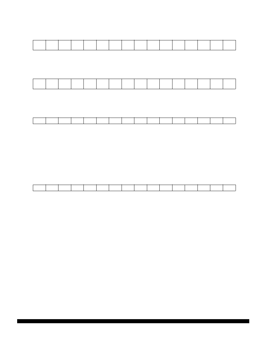
FEE1BAH, FEE2BAH — Flash EEPROM Base Address High Registers
$YFF804, $YFF824
15
14
13
12
11
10
9
8
7
6
5
4
3
2
1
0
00000000
ADDR
23
ADDR
22
ADDR
21
ADDR
20
ADDR
19
ADDR
18
ADDR
17
ADDR
16
RESET:
0
SB
FEE1BAL — Flash EEPROM Base Address Low Register
$YFF806
15
14
13
12
11
10
9
8
7
6
5
4
3
2
1
0
ADDR
15
ADDR
14
00000000000000
RESET:
SB
0
FEE2BAL — Flash EEPROM Base Address Low Register
$YFF826
15
14
13
12
11
10
9
8
7
6
5
4
3
2
1
0
0000000000000000
RESET:
SB
0
FEE1CTL, FEE2CTL — Flash EEPROM Control Register
$YFF808, $YFF828
15
14
13
12
11
10
9
8
7
6
5
4
3
2
1
0
VFPE ERAS LAT ENPE
RESET:
0
F
re
e
sc
a
le
S
e
m
ic
o
n
d
u
c
to
r,
I
Freescale Semiconductor, Inc.
For More Information On This Product,
Go to: www.freescale.com
n
c
..
.
相關PDF資料 |
PDF描述 |
|---|---|
| SPMC916X1CTH16 | 16-BIT, FLASH, 16.78 MHz, MICROCONTROLLER, PQFP120 |
| MC68HCL05J1ADWR2 | 8-BIT, MROM, 2.1 MHz, MICROCONTROLLER, PDSO20 |
| MC68HC05J1AVDWR2 | 8-BIT, MROM, 2.1 MHz, MICROCONTROLLER, PDSO20 |
| MC68HCP11A1CFNE3 | 8-BIT, EEPROM, 3 MHz, MICROCONTROLLER, PQCC52 |
| MC68HLC705KJ1C | 8-BIT, OTPROM, 4 MHz, MICROCONTROLLER, PDIP16 |
相關代理商/技術參數(shù) |
參數(shù)描述 |
|---|---|
| MC92052 | 制造商:MOTOROLA 制造商全稱:Motorola, Inc 功能描述:FTTC User Framer |
| MC92053 | 制造商:MOTOROLA 制造商全稱:Motorola, Inc 功能描述:Quad FTTC Network Framer |
| MC92101CO | 制造商:Rochester Electronics LLC 功能描述:- Bulk |
| MC921G | 制造商:Rochester Electronics LLC 功能描述:- Bulk |
| MC92300 | 制造商:MOTOROLA 制造商全稱:Motorola, Inc 功能描述:VITERBI Decoder for Digital TV |
發(fā)布緊急采購,3分鐘左右您將得到回復。