- 您現(xiàn)在的位置:買賣IC網(wǎng) > PDF目錄69029 > MC916X1CTH16B1 (FREESCALE SEMICONDUCTOR INC) 16-BIT, FLASH, 16.78 MHz, MICROCONTROLLER, PQFP120 PDF資料下載
參數(shù)資料
| 型號: | MC916X1CTH16B1 |
| 廠商: | FREESCALE SEMICONDUCTOR INC |
| 元件分類: | 微控制器/微處理器 |
| 英文描述: | 16-BIT, FLASH, 16.78 MHz, MICROCONTROLLER, PQFP120 |
| 封裝: | QFP-120 |
| 文件頁數(shù): | 13/172頁 |
| 文件大小: | 1200K |
| 代理商: | MC916X1CTH16B1 |
第1頁第2頁第3頁第4頁第5頁第6頁第7頁第8頁第9頁第10頁第11頁第12頁當(dāng)前第13頁第14頁第15頁第16頁第17頁第18頁第19頁第20頁第21頁第22頁第23頁第24頁第25頁第26頁第27頁第28頁第29頁第30頁第31頁第32頁第33頁第34頁第35頁第36頁第37頁第38頁第39頁第40頁第41頁第42頁第43頁第44頁第45頁第46頁第47頁第48頁第49頁第50頁第51頁第52頁第53頁第54頁第55頁第56頁第57頁第58頁第59頁第60頁第61頁第62頁第63頁第64頁第65頁第66頁第67頁第68頁第69頁第70頁第71頁第72頁第73頁第74頁第75頁第76頁第77頁第78頁第79頁第80頁第81頁第82頁第83頁第84頁第85頁第86頁第87頁第88頁第89頁第90頁第91頁第92頁第93頁第94頁第95頁第96頁第97頁第98頁第99頁第100頁第101頁第102頁第103頁第104頁第105頁第106頁第107頁第108頁第109頁第110頁第111頁第112頁第113頁第114頁第115頁第116頁第117頁第118頁第119頁第120頁第121頁第122頁第123頁第124頁第125頁第126頁第127頁第128頁第129頁第130頁第131頁第132頁第133頁第134頁第135頁第136頁第137頁第138頁第139頁第140頁第141頁第142頁第143頁第144頁第145頁第146頁第147頁第148頁第149頁第150頁第151頁第152頁第153頁第154頁第155頁第156頁第157頁第158頁第159頁第160頁第161頁第162頁第163頁第164頁第165頁第166頁第167頁第168頁第169頁第170頁第171頁第172頁
MC68HC916X1
MOTOROLA
MC68HC916X1TS/D
11
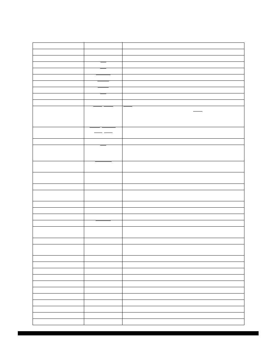
2.5 MCU Signal Function
Table 6 MCU Signal Function
Signal Name
Mnemonic
Function
Address Bus
ADDR[19:0]
20-bit address bus used by CPU16
ADC Analog Input
AN[5:0]
Inputs to ADC multiplexer
Address Strobe
AS
Indicates that a valid address is on the address bus
Bus Grant
BG
Indicates that the MCU has relinquished the bus
Bus Grant Acknowledge
BGACK
Indicates that an external device has assumed bus mastership
Bus Error
BERR
Indicates that a bus error has occurred
Breakpoint
BKPT
Signals a hardware breakpoint to the CPU
Bus Request
BR
Indicates that an external device requires bus mastership
System Clockout
CLKOUT
System clock output
Emulation Mode
Chip-Selects
CSE, CSM
CSE selects external emulation devices at internally-mapped ad-
dresses. It is used to emulate I/O ports. CSM has no function on the
MC68HC916X1. It is driven high if the SCIM is configured for emu-
lation mode.
Chip-Selects
CS10, CS[6:5],
CS3, CS0
Select external devices at programmed addresses
Data Bus
DATA[15:0]
16-bit data bus
Data Strobe
DS
During a read cycle, indicates that an external device should place
valid data on the data bus. During a write cycle, indicates that valid
data is on the data bus.
Data and Size
Acknowledge
DSACK1
Asserted by external devices during asynchronous transfers to in-
dicate receipt of data and width of receiving port
Development Serial In,
Out, Clock
DSI, DSO, DSCLK Serial I/O and clock for background debug mode
External Clock
ECLK
M6800 bus clock output
Crystal Oscillator
EXTAL, XTAL
Connections for clock synthesizer circuit reference; a crystal or an
external oscillator can be used
Function Codes
FC[2:0]
Identify processor state and current address space
Freeze
FREEZE
Indicates that the CPU16 has entered background mode
Instruction Pipeline
IPIPE[1:0]
Indicates instruction pipeline activity
Interrupt Request
IRQ[7:6]
Request interrupt service from the CPU16
Master In Slave Out
MISO
Serial input to SPI in master mode; serial output from SPI in slave
mode
Clock Mode Select
MODCLK
Selects the source and type of system clock
Master Out Slave In
MOSI
Serial output from SPI in master mode; serial input to SPI in slave
mode
Peripheral Chip-Selects
PCS[3:0]
QSPI peripheral chip selects
Port A
PA[7:0]
Port A digital input or output signals
Port B
PB[7:0]
Port B digital input or output signals
Port C
PC[3:0]
Port C digital input/output port signals
Port E
PE1, PE[7:4]
Port E digital I/O port signals
Port F
PF0, PF[7:6]
Port F digital I/O port signals
Port G
PG[7:0]
Port G digital I/O signals
Port GP
PGP[7:0]
GPT digital I/O port signal
Port H
PH[7:0]
Port H digital I/O signal
Port QS
PQS[7:0]
QSM digital I/O port signal
Pulse Accumulator Input
PAI
Input to the GPT pulse accumulator
F
re
e
sc
a
le
S
e
m
ic
o
n
d
u
c
to
r,
I
Freescale Semiconductor, Inc.
For More Information On This Product,
Go to: www.freescale.com
n
c
..
.
相關(guān)PDF資料 |
PDF描述 |
|---|---|
| SPMC916X1CTH16 | 16-BIT, FLASH, 16.78 MHz, MICROCONTROLLER, PQFP120 |
| MC68HCL05J1ADWR2 | 8-BIT, MROM, 2.1 MHz, MICROCONTROLLER, PDSO20 |
| MC68HC05J1AVDWR2 | 8-BIT, MROM, 2.1 MHz, MICROCONTROLLER, PDSO20 |
| MC68HCP11A1CFNE3 | 8-BIT, EEPROM, 3 MHz, MICROCONTROLLER, PQCC52 |
| MC68HLC705KJ1C | 8-BIT, OTPROM, 4 MHz, MICROCONTROLLER, PDIP16 |
相關(guān)代理商/技術(shù)參數(shù) |
參數(shù)描述 |
|---|---|
| MC92052 | 制造商:MOTOROLA 制造商全稱:Motorola, Inc 功能描述:FTTC User Framer |
| MC92053 | 制造商:MOTOROLA 制造商全稱:Motorola, Inc 功能描述:Quad FTTC Network Framer |
| MC92101CO | 制造商:Rochester Electronics LLC 功能描述:- Bulk |
| MC921G | 制造商:Rochester Electronics LLC 功能描述:- Bulk |
| MC92300 | 制造商:MOTOROLA 制造商全稱:Motorola, Inc 功能描述:VITERBI Decoder for Digital TV |
發(fā)布緊急采購,3分鐘左右您將得到回復(fù)。