- 您現在的位置:買賣IC網 > PDF目錄98007 > M44C588 (TEMIC SEMICONDUCTORS) 4-BIT, MROM, 4 MHz, MICROCONTROLLER PDF資料下載
參數資料
| 型號: | M44C588 |
| 廠商: | TEMIC SEMICONDUCTORS |
| 元件分類: | 微控制器/微處理器 |
| 英文描述: | 4-BIT, MROM, 4 MHz, MICROCONTROLLER |
| 文件頁數: | 33/44頁 |
| 文件大小: | 549K |
| 代理商: | M44C588 |
第1頁第2頁第3頁第4頁第5頁第6頁第7頁第8頁第9頁第10頁第11頁第12頁第13頁第14頁第15頁第16頁第17頁第18頁第19頁第20頁第21頁第22頁第23頁第24頁第25頁第26頁第27頁第28頁第29頁第30頁第31頁第32頁當前第33頁第34頁第35頁第36頁第37頁第38頁第39頁第40頁第41頁第42頁第43頁第44頁

M44C588
Preliminary Information
TELEFUNKEN Semiconductors
Rev. A1, 11-Nov-97
39 (44)
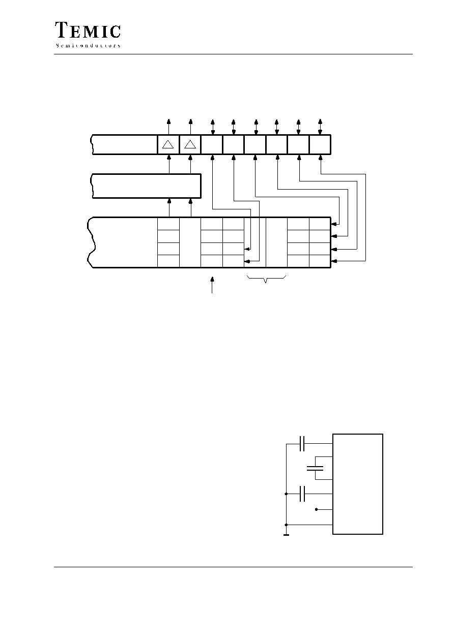
(see table 25). The port data and direction information is
mapped into the LCD shadow register cells SR31 down
to SRn as shown in figure 27. Because each block of 4 I/O
pins only require two register cells (4 bit for data register
and 4 bit for data direction register), only the upper two
cells are used, the upper cell acting as data register and the
one below as the data direction register. For example the
MSBs of these two cells provide the data direction in-
formation for the upper I/O pin.
DDR28 DAT28
Bit 0
Bit 1
Bit 2
Bit 3
XX
X
DDR27 DAT27
DAT26
DDR29 DAT29
DDR30 DAT30
DDR31 DAT31
LCD
data
SR24
SR25
SR26
SR27
SR28
SR29
SR30
SR31
I/O
LCD driver
LCD display buffer
Shadow register
not used
Address pointer
DATx = data of I/O pin Sx
DDRx = direction of I/O pin Sx
DDR26
S24
S25
S26
S27
S28
S29
S30
S31
Figure 27. LCD 32 – 6 segment outputs used as I/O ports
If two I/O pins are used, the upper two cells are used as
data direction and data register and the shadow register
cells below are used for driving the LCD segments. In this
case only the upper two bits are significant for the port and
port data direction (see figure 27 ).
The access to the port direction and data register is identi-
cal to the LCD shadow register read/write access. A data
direction (logical ’1’) bit sets the corresponding I/O pin
into output mode and a logical ’0’ into input mode
3.3
LCD Voltage and Timing
Generator
The LCD voltage generator circuitry boosts the regulated
liquid crystal display voltage (VREG) to the doubled and
tripled voltage components (VEE1, VEE2) required by
multiplexed liquid crystal displays. These voltage levels
are applied to the driver circuitry (see figure 28).
Most low voltage (3 V) LCD panels have a temperature
coefficient of –6 mV/
°C. The temperature compensated
reference for the LCD voltage booster circuitry (VREG),
has the task of meeting this requirement directly, so that
the user gets the best LCD contrast over the full operating
temperature and supply voltage range. The external com-
ponents for the LCD voltage generation (one pump and
two storage capacitors) should be connected to the
mC as
shown in figure 28. For very small LCD panels the capaci-
tor values and charge pumping frequency may be reduced
to save costs and system current. The capacitor values
may be reduced from 100 nF to 47 nF. The user has to con-
nect the
mC and the LCD as it will be in the final product
in order to select the capacitor value. To examine the LCD
driver waveforms, an oscilloscope with a low capacitance
probe should be used.
C1
V
SS
100 nF
V
EE2
C2
V
EE1
V
REG
100 nF
TP
Figure 28. External components
相關PDF資料 |
PDF描述 |
|---|---|
| M44C892 | 4-BIT, MROM, 4 MHz, MICROCONTROLLER, PDSO20 |
| M48T08Y-15PC1 | 0 TIMER(S), REAL TIME CLOCK, PDMA28 |
| M48T08Y-10PC1 | 0 TIMER(S), REAL TIME CLOCK, PDMA28 |
| M48T128Y-70PM1 | 0 TIMER(S), REAL TIME CLOCK, PDIP32 |
| M48T128Y-85PM1 | 0 TIMER(S), REAL TIME CLOCK, PDIP32 |
相關代理商/技術參數 |
參數描述 |
|---|---|
| M44C890 | 制造商:ATMEL 制造商全稱:ATMEL Corporation 功能描述:Low-Current Microcontroller for Wireless Communication |
| M44C890-H | 制造商:ATMEL 制造商全稱:ATMEL Corporation 功能描述:Low-Current Microcontroller for Wireless Communication |
| M44S05K4F1 | 功能描述:汽車連接器 MX44 Terminals RoHS:否 制造商:Amphenol SINE Systems 產品:Contacts 系列:ATP 位置數量: 型式:Female 安裝風格: 端接類型: 觸點電鍍:Nickel |
| M44T332538880MHZ | 制造商:MEC 功能描述: |
| M44T3338880MHZ | 制造商:MEC 功能描述: |
發(fā)布緊急采購,3分鐘左右您將得到回復。