- 您現(xiàn)在的位置:買賣IC網(wǎng) > PDF目錄296349 > M30L0R8000B0ZAQE (STMICROELECTRONICS) 16M X 16 FLASH 1.8V PROM, 85 ns, PBGA88 PDF資料下載
參數(shù)資料
| 型號: | M30L0R8000B0ZAQE |
| 廠商: | STMICROELECTRONICS |
| 元件分類: | PROM |
| 英文描述: | 16M X 16 FLASH 1.8V PROM, 85 ns, PBGA88 |
| 封裝: | 8 X 10 MM, 0.80 MM PITCH, LEAD FREE, TFBGA-88 |
| 文件頁數(shù): | 5/83頁 |
| 文件大?。?/td> | 1569K |
| 代理商: | M30L0R8000B0ZAQE |
第1頁第2頁第3頁第4頁當(dāng)前第5頁第6頁第7頁第8頁第9頁第10頁第11頁第12頁第13頁第14頁第15頁第16頁第17頁第18頁第19頁第20頁第21頁第22頁第23頁第24頁第25頁第26頁第27頁第28頁第29頁第30頁第31頁第32頁第33頁第34頁第35頁第36頁第37頁第38頁第39頁第40頁第41頁第42頁第43頁第44頁第45頁第46頁第47頁第48頁第49頁第50頁第51頁第52頁第53頁第54頁第55頁第56頁第57頁第58頁第59頁第60頁第61頁第62頁第63頁第64頁第65頁第66頁第67頁第68頁第69頁第70頁第71頁第72頁第73頁第74頁第75頁第76頁第77頁第78頁第79頁第80頁第81頁第82頁第83頁
Obsolete
Product(s)
- Obsolete
Product(s)
13/83
M30L0R8000T0, M30L0R8000B0
BUS OPERATIONS
There are six standard bus operations that control
the device. These are Bus Read, Bus Write, Ad-
dress Latch, Output Disable, Standby and Reset.
See Table 3., Bus Operations, for a summary.
Typically glitches of less than 5ns on Chip Enable
or Write Enable are ignored by the memory and do
not affect Bus Write operations.
Bus Read. Bus Read operations are used to out-
put the contents of the Memory Array, the Elec-
tronic Signature, the Status Register and the
Common Flash Interface. Both Chip Enable and
Output Enable must be at VIL in order to perform a
read operation. The Chip Enable input should be
used to enable the device. Output Enable should
be used to gate data onto the output. The data
read depends on the previous command written to
the memory (see Command Interface section).
istics, for details of when the output becomes
valid.
Bus Write. Bus Write operations write Com-
mands to the memory or latch Input Data to be
programmed. A bus write operation is initiated
when Chip Enable and Write Enable are at VIL with
Output Enable at VIH. Commands, Input Data and
Addresses are latched on the rising edge of Write
Enable or Chip Enable, whichever occurs first. The
addresses can also be latched prior to the write
operation by toggling Latch Enable. In this case
the Latch Enable should be tied to VIH during the
bus write operation.
details of the timing requirements.
Address Latch. Address latch operations input
valid addresses. Both Chip enable and Latch En-
able must be at VIL during address latch opera-
tions. The addresses are latched on the rising
edge of Latch Enable.
Output Disable. The outputs are high imped-
ance when the Output Enable is at VIH.
Standby. Standby disables most of the internal
circuitry allowing a substantial reduction of the cur-
rent consumption. The memory is in standby when
Chip Enable and Reset are at VIH. The power con-
sumption is reduced to the standby level IDD3 and
the outputs are set to high impedance, indepen-
dently from the Output Enable or Write Enable in-
puts. If Chip Enable switches to VIH during a
program or erase operation, the device enters
Standby mode when finished.
Reset. During Reset mode the memory is dese-
lected and the outputs are high impedance. The
memory is in Reset mode when Reset is at VIL.
The power consumption is reduced to the Reset
level, independently from the Chip Enable, Output
Enable or Write Enable inputs. If Reset is pulled to
VSS during a Program or Erase, this operation is
aborted and the memory content is no longer valid.
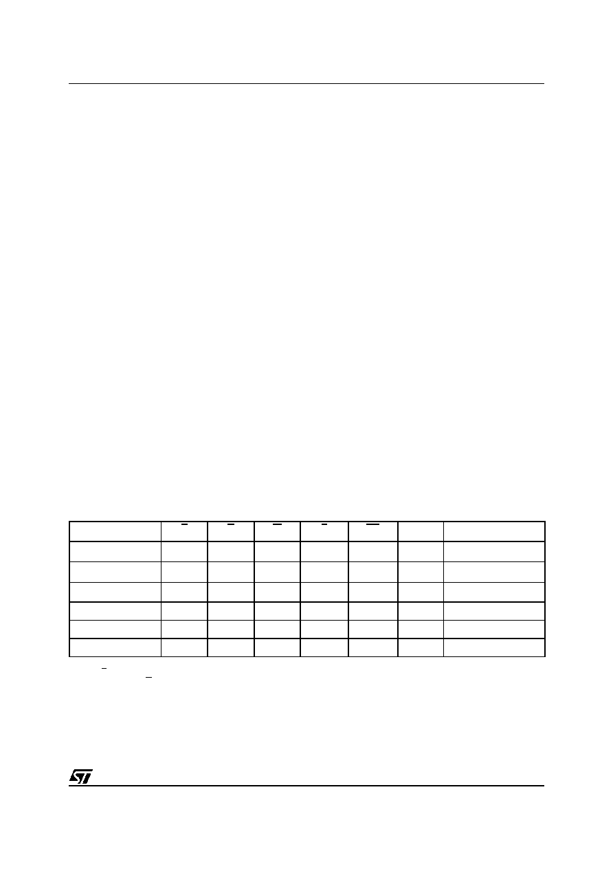
Table 3. Bus Operations
Note: 1. X = Don't care.
2. L can be tied to VIH if the valid address has been previously latched.
3. Depends on G.
4. WAIT signal polarity is configured using the Set Configuration Register command.
Operation
E
G
W
L
RP
WAIT(4)
DQ15-DQ0
Bus Read
VIL
VIH
VIL
(2)
VIH
Data Output
Bus Write
VIL
VIH
VIL
(2)
VIH
Data Input
Address Latch
VIL
X
VIH
VIL
VIH
Data Output or Hi-Z (3)
Output Disable
VIL
VIH
X
VIH
Hi-Z
Standby
VIH
XX
X
VIH
Hi-Z
Reset
X
VIL
Hi-Z
相關(guān)PDF資料 |
PDF描述 |
|---|---|
| M30L0T8000B0ZAQE | 16M X 16 FLASH 1.8V PROM, 85 ns, PBGA88 |
| M31002AMLJ1000.000000MHZ | VCXO, CLOCK, 1000 MHz, LVDS OUTPUT |
| M31016AUMJ1000.000000MHZ | VCXO, CLOCK, 1000 MHz, CMOS OUTPUT |
| M31002AGMJ1000.000000MHZ | VCXO, CLOCK, 1000 MHz, CMOS OUTPUT |
| M31002BMMJ1000.000000MHZ | VCXO, CLOCK, 1000 MHz, CMOS OUTPUT |
相關(guān)代理商/技術(shù)參數(shù) |
參數(shù)描述 |
|---|---|
| M30L0R8000B0ZAQF | 制造商:STMICROELECTRONICS 制造商全稱:STMicroelectronics 功能描述:256 Mbit (16Mb x16, Multiple Bank, Multi-Level, Burst) 1.8V Supply Flash Memory |
| M30L0R8000B0ZAQT | 制造商:STMICROELECTRONICS 制造商全稱:STMicroelectronics 功能描述:256 Mbit (16Mb x16, Multiple Bank, Multi-Level, Burst) 1.8V Supply Flash Memory |
| M30L0R8000T0 | 制造商:STMICROELECTRONICS 制造商全稱:STMicroelectronics 功能描述:256 Mbit (16Mb x16, Multiple Bank, Multi-Level, Burst) 1.8V Supply Flash Memory |
| M30L0R8000T0ZAQ | 制造商:STMICROELECTRONICS 制造商全稱:STMicroelectronics 功能描述:256 Mbit (16Mb x16, Multiple Bank, Multi-Level, Burst) 1.8V Supply Flash Memory |
| M30L0R8000T0ZAQE | 制造商:STMICROELECTRONICS 制造商全稱:STMicroelectronics 功能描述:256 Mbit (16Mb x16, Multiple Bank, Multi-Level, Burst) 1.8V Supply Flash Memory |
發(fā)布緊急采購,3分鐘左右您將得到回復(fù)。