- 您現(xiàn)在的位置:買賣IC網(wǎng) > PDF目錄371862 > HMS77C2001 [General Purpose(2) : ADC/ LED/ SCI/ PWM] PDF資料下載
參數(shù)資料
| 型號(hào): | HMS77C2001 |
| 英文描述: | [General Purpose(2) : ADC/ LED/ SCI/ PWM] |
| 中文描述: | [通用(2):藝術(shù)發(fā)展局/發(fā)光/工商/脈寬調(diào)制] |
| 文件頁(yè)數(shù): | 32/59頁(yè) |
| 文件大?。?/td> | 660K |
| 代理商: | HMS77C2001 |
第1頁(yè)第2頁(yè)第3頁(yè)第4頁(yè)第5頁(yè)第6頁(yè)第7頁(yè)第8頁(yè)第9頁(yè)第10頁(yè)第11頁(yè)第12頁(yè)第13頁(yè)第14頁(yè)第15頁(yè)第16頁(yè)第17頁(yè)第18頁(yè)第19頁(yè)第20頁(yè)第21頁(yè)第22頁(yè)第23頁(yè)第24頁(yè)第25頁(yè)第26頁(yè)第27頁(yè)第28頁(yè)第29頁(yè)第30頁(yè)第31頁(yè)當(dāng)前第32頁(yè)第33頁(yè)第34頁(yè)第35頁(yè)第36頁(yè)第37頁(yè)第38頁(yè)第39頁(yè)第40頁(yè)第41頁(yè)第42頁(yè)第43頁(yè)第44頁(yè)第45頁(yè)第46頁(yè)第47頁(yè)第48頁(yè)第49頁(yè)第50頁(yè)第51頁(yè)第52頁(yè)第53頁(yè)第54頁(yè)第55頁(yè)第56頁(yè)第57頁(yè)第58頁(yè)第59頁(yè)
HMS77C2000/2001
Nov. 2002 Ver 1.1
29
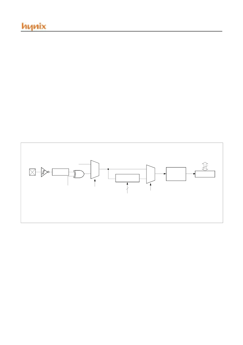
11. TIMER0 MODULE AND TMR0 REGISTER
The Timer0 module has the following features:
- 8-bit timer/counter register, TMR0
- Readable and writable
- 8-bit software programmable prescaler
- Internal or external clock select
- Edge select for external clock
Figure 11-1 is a simplified block diagram of the Timer0
module.
Timer mode is selected by clearing the T0CS bit (OP-
TION<5>). In timer mode, the Timer0 module will incre-
ment every instruction cycle (without prescaler). If TMR0
register is written, the increment is inhibited for the follow-
ing two instruction cycles (Figure 11-2 and Figure 11-3).
The user can work around this by writing an adjusted value
to the TMR0 register.
Counter mode is selected by setting the T0CS bit (OP-
TION<5>). In this mode, Timer0 will increment either on
every rising or falling edge of pin T0CKI. The T0SE bit
(OPTION<4>) determines the source edge. Clearing the
T0SE bit selects the rising edge. Restrictions on the exter-
nal clock input are discussed in detail in Section 6.1.
The prescaler may be used by either the Timer0 module or
the Watchdog Timer, but not both. The prescaler assign-
ment is controlled in software by the control bit PSA (OP-
TION<3>). Clearing the PSA bit will assign the prescaler
to Timer0. The prescaler is not readable or writable. When
the prescaler is assigned to the Timer0 module, prescale
values of 1:2, 1:4,..., 1:256 are selectable. Section 6.2 de-
tails the operation of the prescaler.
A summary of registers associated with the Timer0 module
is found in Table 6-1.
FIGURE 11-1 TIMER0 BLOCK DIAGRAM
F
OSC
/4
1
UP2/EC0
pin
0
Sync with
Internal
Clocks
TMR0 reg
8
Data bus
(2 T
CY
delay)
T0SE
T0CS
1
MUX
0
1
MUX
PSA
1
PS
OUT
PS
OUT
Sync
Programmable
Prescaler
3
PS2, PS1, PS0
1
Note 1 : Bits T0CS, T0SE, PSA, PS2, PS1 and PS0 are located in the OPTION register.
2 : The prescaler is shared with the watchdog timer.
Noise
Filter
相關(guān)PDF資料 |
PDF描述 |
|---|---|
| HMS81004 | REMOTE CONTROLLER |
| HMS81008 | siHYNIX SEMICONDUCTOR 8-BIT SINGLE-CHIP MICROCONTROLLERS |
| HMS81016 | REMOTE CONTROLLER |
| HMS81020ET | REMOTE CONTROLLER |
| HMS81024 | REMOTE CONTROLLER |
相關(guān)代理商/技術(shù)參數(shù) |
參數(shù)描述 |
|---|---|
| HMS81004 | 制造商:未知廠家 制造商全稱:未知廠家 功能描述:REMOTE CONTROLLER |
| HMS81004E | 制造商:HYNIX 制造商全稱:Hynix Semiconductor 功能描述:HYNIX SEMICONDUCTOR 8-BIT SINGLE-CHIP MICROCONTROLLERS |
| HMS81008 | 制造商:未知廠家 制造商全稱:未知廠家 功能描述:REMOTE CONTROLLER |
| HMS81008E | 制造商:HYNIX 制造商全稱:Hynix Semiconductor 功能描述:HYNIX SEMICONDUCTOR 8-BIT SINGLE-CHIP MICROCONTROLLERS |
| HMS81016 | 制造商:未知廠家 制造商全稱:未知廠家 功能描述:REMOTE CONTROLLER |
發(fā)布緊急采購(gòu),3分鐘左右您將得到回復(fù)。