- 您現(xiàn)在的位置:買賣IC網(wǎng) > PDF目錄371862 > HMS77C2001 [General Purpose(2) : ADC/ LED/ SCI/ PWM] PDF資料下載
參數(shù)資料
| 型號: | HMS77C2001 |
| 英文描述: | [General Purpose(2) : ADC/ LED/ SCI/ PWM] |
| 中文描述: | [通用(2):藝術(shù)發(fā)展局/發(fā)光/工商/脈寬調(diào)制] |
| 文件頁數(shù): | 30/59頁 |
| 文件大?。?/td> | 660K |
| 代理商: | HMS77C2001 |
第1頁第2頁第3頁第4頁第5頁第6頁第7頁第8頁第9頁第10頁第11頁第12頁第13頁第14頁第15頁第16頁第17頁第18頁第19頁第20頁第21頁第22頁第23頁第24頁第25頁第26頁第27頁第28頁第29頁當(dāng)前第30頁第31頁第32頁第33頁第34頁第35頁第36頁第37頁第38頁第39頁第40頁第41頁第42頁第43頁第44頁第45頁第46頁第47頁第48頁第49頁第50頁第51頁第52頁第53頁第54頁第55頁第56頁第57頁第58頁第59頁

HMS77C2000/2001
Nov. 2002 Ver 1.1
27
10.4 I/O PROGRAMMING CONSIDERATIONS
10.4.1 BI-DIRECTIONAL I/O PORTS
Some instructions operate internally as read followed by
write operations. The
BCF
and
BSF
instructions, for exam-
ple, read the entire port into the CPU, execute the bit oper-
ation and re-write the result. Caution must be used when
these instructions are applied to a port where one or more
pins are used as input/outputs. For example, a
BSF
opera-
tion on bit5 of UPIO will cause all eight bits of UPIO to be
read into the CPU, bit5 to be set and the UPIO value to be
written to the output latches. If another bit of UPIO is used
as a bidirectional I/O pin (say bit0) and it is defined as an
input at this time, the input signal present on the pin itself
would be read into the CPU and rewritten to the data latch
of this particular pin, overwriting the previous content. As
long as the pin stays in the input mode, no problem occurs.
However, if bit0 is switched into output mode later on, the
content of the data latch may now be unknown.
Example 5-1 shows the effect of two sequential read-mod-
ify-write instructions (e.g.,
BCF
,
BSF
, etc.) on an I/O port.
pin actively outputting a high or a low should not be driven
from external devices at the same time in order to change
the level on this pin (“wired-or”, “wired-and”). The result-
ing high output currents may damage the chip.
EXAMPLE 5-1: READ-MODIFY-WRITE INSTRUC-
TIONS ON AN I/O PORT
;Initial UPIO Settings
;UPIO<5:3> Inputs
;UPIO<2:0> Outputs
;
;
;
BCF UPIO, 5 ;--01 -ppp --11 pppp
BCF UPIO, 4 ;--10 -ppp --11 pppp
MOVLW 007h ;
TRIS UPIO ;--10 -ppp --11 pppp
;
;Note that the user may have expected the
;pin values to be --00 pppp. The 2nd BCF
;caused UP5 to be latched as the pin value
(High).
UPIO latch UPIO pins
---------- ----------
10.4.2 SUCCESSIVE OPERATIONS ON I/O
PORTS
The actual write to an I/O port happens at the end of an in-
struction cycle, whereas for reading, the data must be valid
at the beginning of the instruction cycle Figure 10-2).
Therefore, care must be exercised if a write followed by a
read operation is carried out on the same I/O port. The se-
quence of instructions should allow the pin voltage to sta-
bilize (load dependent) before the next instruction, which
causes that file to be read into the CPU, is executed. Oth-
erwise, the previous state of that pin may be read into the
CPU rather than the new state. When in doubt, it is better
to separate these instructions with a
NOP
or another in-
struction not accessing this I/O port.
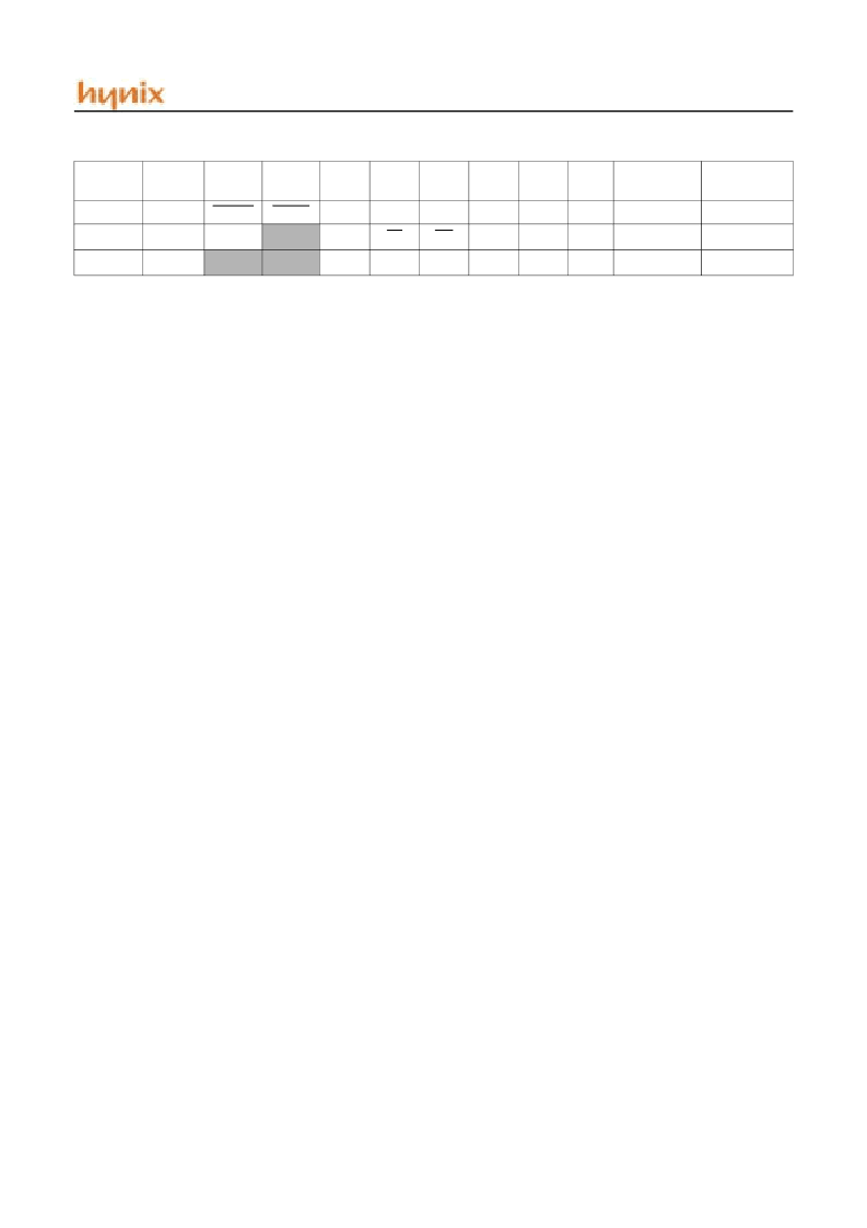
N/A
OPTION
GPWU
GPPU
T0CS
T0SE
PSA
PS2
PS1
PS0
1111 1111
1111 1111
03
H
STATUS
UPWUF
PA0
T0
PD
Z
DC
C
0001 1xxx
q00q quuu
1
06
H
UPIO
UP5
UP4
UP3
UP2
UP1
UP0
11xx xxxx
11uu uuuu
1. If reset was due to wake-up on change, then bit 7 = 1. All other resets will cause bit 7 = 0
Address
Name
Bit7
Bit6
Bit5
Bit4
Bit3
Bit2
Bit1
Bit0
Power-On
Reset
All other
Resets
TABLE 10-1 SUMMARY OF PORT REGISTERS
Legend: Shaded boxes = unimplemented or unused, - = unimplemented, read as ‘0’, x = unknown, u = unchanged.
相關(guān)PDF資料 |
PDF描述 |
|---|---|
| HMS81004 | REMOTE CONTROLLER |
| HMS81008 | siHYNIX SEMICONDUCTOR 8-BIT SINGLE-CHIP MICROCONTROLLERS |
| HMS81016 | REMOTE CONTROLLER |
| HMS81020ET | REMOTE CONTROLLER |
| HMS81024 | REMOTE CONTROLLER |
相關(guān)代理商/技術(shù)參數(shù) |
參數(shù)描述 |
|---|---|
| HMS81004 | 制造商:未知廠家 制造商全稱:未知廠家 功能描述:REMOTE CONTROLLER |
| HMS81004E | 制造商:HYNIX 制造商全稱:Hynix Semiconductor 功能描述:HYNIX SEMICONDUCTOR 8-BIT SINGLE-CHIP MICROCONTROLLERS |
| HMS81008 | 制造商:未知廠家 制造商全稱:未知廠家 功能描述:REMOTE CONTROLLER |
| HMS81008E | 制造商:HYNIX 制造商全稱:Hynix Semiconductor 功能描述:HYNIX SEMICONDUCTOR 8-BIT SINGLE-CHIP MICROCONTROLLERS |
| HMS81016 | 制造商:未知廠家 制造商全稱:未知廠家 功能描述:REMOTE CONTROLLER |
發(fā)布緊急采購,3分鐘左右您將得到回復(fù)。