- 您現(xiàn)在的位置:買賣IC網(wǎng) > PDF目錄385707 > PD784976A (NEC Corp.) 16-Bit Single-Chip Microcontroller PDF資料下載
參數(shù)資料
| 型號: | PD784976A |
| 廠商: | NEC Corp. |
| 英文描述: | 16-Bit Single-Chip Microcontroller |
| 中文描述: | 16位單片機 |
| 文件頁數(shù): | 366/400頁 |
| 文件大小: | 2023K |
| 代理商: | PD784976A |
第1頁第2頁第3頁第4頁第5頁第6頁第7頁第8頁第9頁第10頁第11頁第12頁第13頁第14頁第15頁第16頁第17頁第18頁第19頁第20頁第21頁第22頁第23頁第24頁第25頁第26頁第27頁第28頁第29頁第30頁第31頁第32頁第33頁第34頁第35頁第36頁第37頁第38頁第39頁第40頁第41頁第42頁第43頁第44頁第45頁第46頁第47頁第48頁第49頁第50頁第51頁第52頁第53頁第54頁第55頁第56頁第57頁第58頁第59頁第60頁第61頁第62頁第63頁第64頁第65頁第66頁第67頁第68頁第69頁第70頁第71頁第72頁第73頁第74頁第75頁第76頁第77頁第78頁第79頁第80頁第81頁第82頁第83頁第84頁第85頁第86頁第87頁第88頁第89頁第90頁第91頁第92頁第93頁第94頁第95頁第96頁第97頁第98頁第99頁第100頁第101頁第102頁第103頁第104頁第105頁第106頁第107頁第108頁第109頁第110頁第111頁第112頁第113頁第114頁第115頁第116頁第117頁第118頁第119頁第120頁第121頁第122頁第123頁第124頁第125頁第126頁第127頁第128頁第129頁第130頁第131頁第132頁第133頁第134頁第135頁第136頁第137頁第138頁第139頁第140頁第141頁第142頁第143頁第144頁第145頁第146頁第147頁第148頁第149頁第150頁第151頁第152頁第153頁第154頁第155頁第156頁第157頁第158頁第159頁第160頁第161頁第162頁第163頁第164頁第165頁第166頁第167頁第168頁第169頁第170頁第171頁第172頁第173頁第174頁第175頁第176頁第177頁第178頁第179頁第180頁第181頁第182頁第183頁第184頁第185頁第186頁第187頁第188頁第189頁第190頁第191頁第192頁第193頁第194頁第195頁第196頁第197頁第198頁第199頁第200頁第201頁第202頁第203頁第204頁第205頁第206頁第207頁第208頁第209頁第210頁第211頁第212頁第213頁第214頁第215頁第216頁第217頁第218頁第219頁第220頁第221頁第222頁第223頁第224頁第225頁第226頁第227頁第228頁第229頁第230頁第231頁第232頁第233頁第234頁第235頁第236頁第237頁第238頁第239頁第240頁第241頁第242頁第243頁第244頁第245頁第246頁第247頁第248頁第249頁第250頁第251頁第252頁第253頁第254頁第255頁第256頁第257頁第258頁第259頁第260頁第261頁第262頁第263頁第264頁第265頁第266頁第267頁第268頁第269頁第270頁第271頁第272頁第273頁第274頁第275頁第276頁第277頁第278頁第279頁第280頁第281頁第282頁第283頁第284頁第285頁第286頁第287頁第288頁第289頁第290頁第291頁第292頁第293頁第294頁第295頁第296頁第297頁第298頁第299頁第300頁第301頁第302頁第303頁第304頁第305頁第306頁第307頁第308頁第309頁第310頁第311頁第312頁第313頁第314頁第315頁第316頁第317頁第318頁第319頁第320頁第321頁第322頁第323頁第324頁第325頁第326頁第327頁第328頁第329頁第330頁第331頁第332頁第333頁第334頁第335頁第336頁第337頁第338頁第339頁第340頁第341頁第342頁第343頁第344頁第345頁第346頁第347頁第348頁第349頁第350頁第351頁第352頁第353頁第354頁第355頁第356頁第357頁第358頁第359頁第360頁第361頁第362頁第363頁第364頁第365頁當前第366頁第367頁第368頁第369頁第370頁第371頁第372頁第373頁第374頁第375頁第376頁第377頁第378頁第379頁第380頁第381頁第382頁第383頁第384頁第385頁第386頁第387頁第388頁第389頁第390頁第391頁第392頁第393頁第394頁第395頁第396頁第397頁第398頁第399頁第400頁
366
User
’
s Manual U15017EJ2V0UD
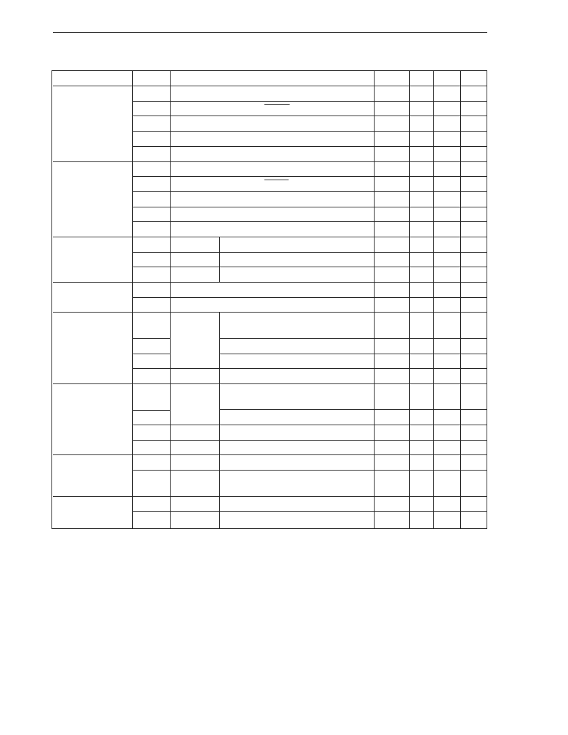
CHAPTER 21 ELECTRICAL SPECIFICATIONS
DC Characteristics (T
A
=
40 to +85
°
C, V
DD
= AV
DD
= 4.5 to 5.5 V, V
SS
= AV
SS
= 0 V) (1/3)
Parameter
Symbol
Conditions
MIN.
TYP.
MAX.
Unit
Input voltage, low
V
IL1
P00 to P03, P10 to P17, P26, P40 to P47, P61
0
0.3V
DD
V
V
IL2
P20, P63 to P67, X1, X2, RESET
0
0.2V
DD
V
V
IL3
P25, P27, P55
Note 1
, P57
Note 1
, P60, P62
0
0.1V
DD
+ 0.4
V
V
IL4
P50 to P57 (N-ch open drain)
0
0.3V
DD
V
V
IL5
P70 to P77, P80 to P87, P90 to P97 (P-ch open drain)
V
DD
35
0.3V
DD
V
Input voltage, high
V
IH1
P00 to P03, P10 to P17, P26, P40 to P47, P61
0.7V
DD
V
DD
V
V
IH2
P20, P63 to P67, X1, X2, RESET
0.8V
DD
V
DD
V
V
IH3
P25, P27, P55
Note 1
, P57
Note 1
, P60, P62
0.3V
DD
+ 0.7
V
DD
V
V
IH4
P50 to P57 (N-ch open drain)
0.7V
DD
12
V
V
IH5
P70 to P77, P80 to P87, P90 to P97 (P-ch open drain)
0.7V
DD
V
DD
V
Output voltage, low
V
OL1
I
OL
= 1.6 mA P20, P25 to P27, P60 to P67
0.4
V
V
OL2
I
OL
= 10 mA
P40 to P47
1.5
V
V
OL3
I
OL
= 15 mA
P50 to P57
2.0
V
Output voltage, high
V
OH1
I
OH
=
1 mA
V
DD
1.0
V
V
OH2
I
OH
=
100
μ
A
V
DD
0.5
V
Input leakage
current, low
I
LIL1
V
I
= 0 V
For pins other than P50 to P57, P70 to
P77, P80 to P87, P90 to P97, X1, and X2
10
μ
A
I
LIL2
X1, X2
20
μ
A
I
LIL3
P50 to P57
10
Note 2
μ
A
I
LIL4
V
I
=
35 V
P70 to P77, P80 to P87, P90 to P97
10
μ
A
Input leakage
current, high
I
LIH1
V
I
= V
DD
For pins other than P50 to P57, P70 to
P77, P80 to P87, P90 to P97, X1, and X2
10
μ
A
I
LIH2
X1, X2
20
μ
A
I
LIH3
V
I
= 12 V
P50 to P57
10
μ
A
I
LIH4
V
I
= V
DD
P70 to P77, P80 to P87, P90 to P97
10
μ
A
Output leakage
current, low
Note 3
I
LOL1
V
O
= 0 V
10
μ
A
I
LOL2
V
O
= V
LOAD
= P70 to P77, P80 to P87, P90 to P97,
35 V
P100 to P107, FIP0 to FIP15
10
μ
A
Output leakage
current, high
Note 3
I
LOH1
V
O
= V
DD
10
μ
I
LOH2
V
O
= 12 V
P50 to P57
10
μ
A
Notes 1.
High-level and low-level input voltages for P55 and P57 apply to V
IH3
and V
IL3
only when SIO2 is used.
They are V
IH4
and V
IL4
when the port is used.
2.
When pull-up resistors are not connected to P50 to P57 (specified by a mask option), a low-level input
leakage current of
200
μ
A (MAX.) flows for only 2 clocks after a read instruction has been executed
to port 5 (P50 to P57). At times other than this 2-clock interval, a
10
μ
A (MAX.) current flows.
3.
The current flowing to on-chip pull-up and pull-down resistors is not included.
Remark
Unless otherwise specified, the characteristics of alternate-function pins are the same as those of port
pins.
相關PDF資料 |
PDF描述 |
|---|---|
| PDA17-VS20-102AK | 17 mm Rotary Potentiometer |
| PDA17-AN25-102AF | 17 mm Rotary Potentiometer |
| PDA17-AN25-102AK | 17 mm Rotary Potentiometer |
| PDA17-AN25-102BF | 17 mm Rotary Potentiometer |
| PDA17-AN25-102BK | 17 mm Rotary Potentiometer |
相關代理商/技術參數(shù) |
參數(shù)描述 |
|---|---|
| PD7869 | 制造商:未知廠家 制造商全稱:未知廠家 功能描述:Optoelectronic |
| PD78F0134 | 制造商:NEC 制造商全稱:NEC 功能描述:8-Bit Single-Chip Microcontrollers |
| PD78F0134(A) | 制造商:NEC 制造商全稱:NEC 功能描述:8-Bit Single-Chip Microcontrollers |
| PD78F0134(A1) | 制造商:NEC 制造商全稱:NEC 功能描述:8-Bit Single-Chip Microcontrollers |
| PD78F0134A | 制造商:NEC 制造商全稱:NEC 功能描述:8-Bit Single-Chip Microcontrollers |
發(fā)布緊急采購,3分鐘左右您將得到回復。