- 您現在的位置:買賣IC網 > PDF目錄69025 > MC68349FT16 (MOTOROLA INC) 32-BIT, MICROCONTROLLER, PQFP16 PDF資料下載
參數資料
| 型號: | MC68349FT16 |
| 廠商: | MOTOROLA INC |
| 元件分類: | 微控制器/微處理器 |
| 英文描述: | 32-BIT, MICROCONTROLLER, PQFP16 |
| 封裝: | PLASTIC, QFP-160 |
| 文件頁數: | 324/420頁 |
| 文件大?。?/td> | 1645K |
| 代理商: | MC68349FT16 |
第1頁第2頁第3頁第4頁第5頁第6頁第7頁第8頁第9頁第10頁第11頁第12頁第13頁第14頁第15頁第16頁第17頁第18頁第19頁第20頁第21頁第22頁第23頁第24頁第25頁第26頁第27頁第28頁第29頁第30頁第31頁第32頁第33頁第34頁第35頁第36頁第37頁第38頁第39頁第40頁第41頁第42頁第43頁第44頁第45頁第46頁第47頁第48頁第49頁第50頁第51頁第52頁第53頁第54頁第55頁第56頁第57頁第58頁第59頁第60頁第61頁第62頁第63頁第64頁第65頁第66頁第67頁第68頁第69頁第70頁第71頁第72頁第73頁第74頁第75頁第76頁第77頁第78頁第79頁第80頁第81頁第82頁第83頁第84頁第85頁第86頁第87頁第88頁第89頁第90頁第91頁第92頁第93頁第94頁第95頁第96頁第97頁第98頁第99頁第100頁第101頁第102頁第103頁第104頁第105頁第106頁第107頁第108頁第109頁第110頁第111頁第112頁第113頁第114頁第115頁第116頁第117頁第118頁第119頁第120頁第121頁第122頁第123頁第124頁第125頁第126頁第127頁第128頁第129頁第130頁第131頁第132頁第133頁第134頁第135頁第136頁第137頁第138頁第139頁第140頁第141頁第142頁第143頁第144頁第145頁第146頁第147頁第148頁第149頁第150頁第151頁第152頁第153頁第154頁第155頁第156頁第157頁第158頁第159頁第160頁第161頁第162頁第163頁第164頁第165頁第166頁第167頁第168頁第169頁第170頁第171頁第172頁第173頁第174頁第175頁第176頁第177頁第178頁第179頁第180頁第181頁第182頁第183頁第184頁第185頁第186頁第187頁第188頁第189頁第190頁第191頁第192頁第193頁第194頁第195頁第196頁第197頁第198頁第199頁第200頁第201頁第202頁第203頁第204頁第205頁第206頁第207頁第208頁第209頁第210頁第211頁第212頁第213頁第214頁第215頁第216頁第217頁第218頁第219頁第220頁第221頁第222頁第223頁第224頁第225頁第226頁第227頁第228頁第229頁第230頁第231頁第232頁第233頁第234頁第235頁第236頁第237頁第238頁第239頁第240頁第241頁第242頁第243頁第244頁第245頁第246頁第247頁第248頁第249頁第250頁第251頁第252頁第253頁第254頁第255頁第256頁第257頁第258頁第259頁第260頁第261頁第262頁第263頁第264頁第265頁第266頁第267頁第268頁第269頁第270頁第271頁第272頁第273頁第274頁第275頁第276頁第277頁第278頁第279頁第280頁第281頁第282頁第283頁第284頁第285頁第286頁第287頁第288頁第289頁第290頁第291頁第292頁第293頁第294頁第295頁第296頁第297頁第298頁第299頁第300頁第301頁第302頁第303頁第304頁第305頁第306頁第307頁第308頁第309頁第310頁第311頁第312頁第313頁第314頁第315頁第316頁第317頁第318頁第319頁第320頁第321頁第322頁第323頁當前第324頁第325頁第326頁第327頁第328頁第329頁第330頁第331頁第332頁第333頁第334頁第335頁第336頁第337頁第338頁第339頁第340頁第341頁第342頁第343頁第344頁第345頁第346頁第347頁第348頁第349頁第350頁第351頁第352頁第353頁第354頁第355頁第356頁第357頁第358頁第359頁第360頁第361頁第362頁第363頁第364頁第365頁第366頁第367頁第368頁第369頁第370頁第371頁第372頁第373頁第374頁第375頁第376頁第377頁第378頁第379頁第380頁第381頁第382頁第383頁第384頁第385頁第386頁第387頁第388頁第389頁第390頁第391頁第392頁第393頁第394頁第395頁第396頁第397頁第398頁第399頁第400頁第401頁第402頁第403頁第404頁第405頁第406頁第407頁第408頁第409頁第410頁第411頁第412頁第413頁第414頁第415頁第416頁第417頁第418頁第419頁第420頁
11-6
MC68349 USER'S MANUAL
MOTOROLA
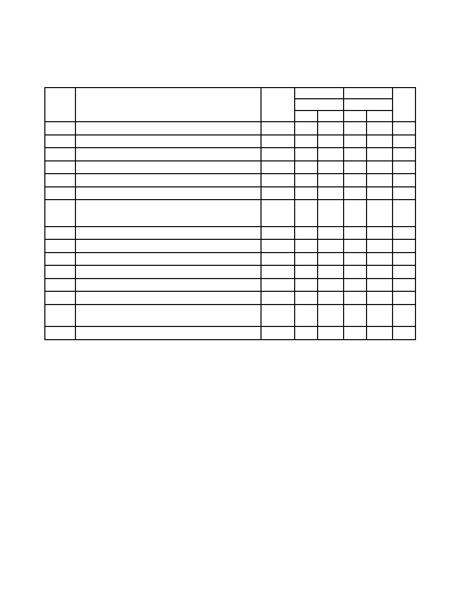
11.6 AC ELECTRICAL SPECIFICATIONS CONTROL TIMING (See notes (a), (b),
and (c) corresponding to part operation, GND = 0 Vdc, TA = 0 to 70
°C; see numbered notes)
3.3 V or 5.0 V
5.0 V
16.78 MHz
25.16 MHz
Num.
Characteristic
Symbol
Min
Max
Min
Max
Unit
System Frequency1
fsys
dc
16.78
dc
25.16
MHz
Crystal Frequency
fXTAL
25
50
25
50
kHz
On-Chip VCO System Frequency
fsys
0.13
16.78
0.13
25.16
MHz
On-Chip VCO Frequency Range
fVCO
0.1
33.5
0.1
50.3
MHz
External Clock Operation
fsys
0
16
0
25
MHz
PLL Start-up Time2
trc
—
20
—
20
ms
Limp Mode Clock Frequency 3
SYNCR X-bit = 0
SYNCR X-bit = 1
flimp
—
fsys/2
fsys
—
fsys/2
fsys
kHz
CLKOUT stability 4
CLK
–1
+1
–1
+1
%
15
CLKOUT Period in Crystal Mode
tcyc
59.6
—
40
—
ns
1B6
External Clock Input Period
tEXTcyc 62.5
—
40
—
ns
1C 7
External Clock Input Period with PLL
tEXTcyc 62.5
—
40
—
ns
2,3 8
CLKOUT Pulse Width in Crystal Mode
tCW
28
—
19
—
ns
2B, 3B9 CLKOUT Pulse Width in External Mode
tEXTCW
28
—
18
—
ns
2C,
3C 10
CLKOUT Pulse Width in External w/PLL Mode
tEXTCW
31
—
20
—
ns
4,5
CLKOUT Rise and Fall Times
tCrf
—
5
—
4
ns
NOTES:
(a) The 16.78-MHz @ 3.3 V
±0.3 V specifications are preliminary and apply to the MC68349V.
(b) The 16.78-MHz @ 5.0 V
±5% specifications are preliminary and apply to the MC68349.
(c) The 25.16 MHz @ 5.0 V
±5% specifications are preliminary and apply to the MC68349.
1.
All internal registers retain data at 0 Hz.
2.
Assumes that a stable VCCSYN is applied, that an external filter capacitor with a value of 0.1 F is attached to
the XFC pin, and that the crystal oscillator is stable. Lock time is measured from power-up to RESET release.
This specification also applies to the period required for PLL lock after changing the W and Y frequency control
bits in the synthesizer control register (SYNCR) while the PLL is running, and to the period required for the clock
to lock after exiting LPSTOP.
3.
Determined by the initial control voltage applied to the on-chip VCO. The X-bit in the SYNCR controls a divide -
by-two scalar on the system clock output.
4.
CLKOUT stability is the average deviation from programmed frequency measured at maximum f sys.
Measurement is made with a stable external clock input applied using the PLL.
5.
All crystal mode clock specifications are based on using a 32.768-kHz crystal for the input.
6.
When using the external clock input mode (MODCK reset value = 0 V), the minimum allowable t EXTcyc period
will be reduced when the duty cycle of the signal applied to EXTAL exceeds 5% tolerance. The relationship
between external clock input duty cycle and minimum t EXTcyc is expressed:
Minimum tEXTcyc period = minimum tEXTCW / (50% – external clock input duty cycle tolerance).
Minimum external clock low and high times are based on a 45% duty cycle.
7.
When using the external clock input mode with the PLL (MODCK reset value = 0 V), the external clock input duty
cycle can be at minimum 20% to produce a CLKOUT with a 50% duty cycle.
8.
For crystal mode operation, the minimum CLKOUT pulse width is based on a 47% duty cycle.
相關PDF資料 |
PDF描述 |
|---|---|
| MC68349FT25 | 32-BIT, MICROCONTROLLER, PQFP16 |
| MC68356CZP25 | 3 CHANNEL(S), 115K bps, SERIAL COMM CONTROLLER, PBGA357 |
| MC68356ZP25 | 3 CHANNEL(S), 115K bps, SERIAL COMM CONTROLLER, PBGA357 |
| MC6840L | 3 TIMER(S), PROGRAMMABLE TIMER, CDIP28 |
| MC68A40L | 3 TIMER(S), PROGRAMMABLE TIMER, CDIP28 |
相關代理商/技術參數 |
參數描述 |
|---|---|
| MC68349FT25A | 制造商:Motorola Inc 功能描述: |
| MC68349V | 制造商:MOTOROLA 制造商全稱:Motorola, Inc 功能描述:HIGH PERFORMANCE INTEGRATED PROCESSOR |
| MC6835 | 制造商:FREESCALE 制造商全稱:Freescale Semiconductor, Inc 功能描述:8-BIT MPUS, 8-BIT MCUS, 8-BIT PERIPHERALS |
| MC68360 | 制造商:MOTOROLA 制造商全稱:Motorola, Inc 功能描述:QUad Integrated Communications Controller Users Manual |
| MC68360AD | 制造商:FREESCALE 制造商全稱:Freescale Semiconductor, Inc 功能描述:MC68360 QUad Integrated Communication Controller (QUICCa?¢) |
發(fā)布緊急采購,3分鐘左右您將得到回復。