- 您現(xiàn)在的位置:買賣IC網(wǎng) > PDF目錄293971 > 5962D1022901QXC 64M X 40 SYNCHRONOUS DRAM, 5.4 ns, CQFP128 PDF資料下載
參數(shù)資料
| 型號: | 5962D1022901QXC |
| 元件分類: | DRAM |
| 英文描述: | 64M X 40 SYNCHRONOUS DRAM, 5.4 ns, CQFP128 |
| 封裝: | CERAMIC, QFP-128 |
| 文件頁數(shù): | 41/68頁 |
| 文件大小: | 1475K |
| 代理商: | 5962D1022901QXC |
第1頁第2頁第3頁第4頁第5頁第6頁第7頁第8頁第9頁第10頁第11頁第12頁第13頁第14頁第15頁第16頁第17頁第18頁第19頁第20頁第21頁第22頁第23頁第24頁第25頁第26頁第27頁第28頁第29頁第30頁第31頁第32頁第33頁第34頁第35頁第36頁第37頁第38頁第39頁第40頁當(dāng)前第41頁第42頁第43頁第44頁第45頁第46頁第47頁第48頁第49頁第50頁第51頁第52頁第53頁第54頁第55頁第56頁第57頁第58頁第59頁第60頁第61頁第62頁第63頁第64頁第65頁第66頁第67頁第68頁
46
Notes:
* For devices procured with a total ionizing dose tolerance guarantee, the post-irradiation performance is guaranteed at 25oC per MIL-STD-883 Method 1019,
Condition A up to the maximum TID level procured.
1. All voltages referenced to VSS.
2. Measured only for initial qualification and after process or design change that could affect this parameter.
3. IDD is dependent on output loading and cycle rates. Specified values are obtained with minimum cycle time and the outputs open.
4. The minimum specifications are used only to indicate cycle time at which proper operation over the full temperature range
(–40°C ≤ TC ≤ 105°C) is ensured.
5. An initial pause of 100μs is required after power-up, followed by two AUTO REFRESH commands, before proper device operation is ensured. (VDD and VDDQ
must be powered up simultaneously. VSS and VSSQ must be at same potential.) The two AUTO REFRESH command wake-ups should be repeated any time the
tREF refresh requirement is exceeded.
6. AC characteristics assume tT = 1ns, supplied as a design limit, neither tested nor guaranteed.
7. In addition to meeting the transition rate specification, the clock and CKE must transit between VIH and VIL (or between VIL and VIH) in a monotonic manner.
8. Outputs measured at 1.5V with equivalent load:
9. AC timing and IDD tests have VIL = 0V and VIH = 3V, with timing referenced to 1.5Vcrossover point. If the input transition time is longer than 1ns, then the
timing is referenced at VIL (MAX) and VIH (MIN) and no longer at the 1.5V crossover point.
10. Other input signals are allowed to transition no more than once every two clocks and are otherwise at valid VIH or VIL levels.
11. IDD specifications are tested after the device is properly initialized.
12. The IDD current will increase or decrease in a proportional amount by the amount the frequency is altered for the test condition.
13. Address transitions average one transition every two clocks.
14. The clock frequency must remain constant (stable clock is defined as a signal cycling within timing constraints specified for the clock pin) during access or
precharge states (READ, WRITE, including tWR, and PRECHARGE commands). CKE may be used to reduce the data rate.
15. CL = 2, tCK = 7.5ns.
16. CKE is HIGH during refresh command period tRFC (MIN) else CKE is LOW. The IDD6 limit is actually a nominal value and does not result in a fail value.
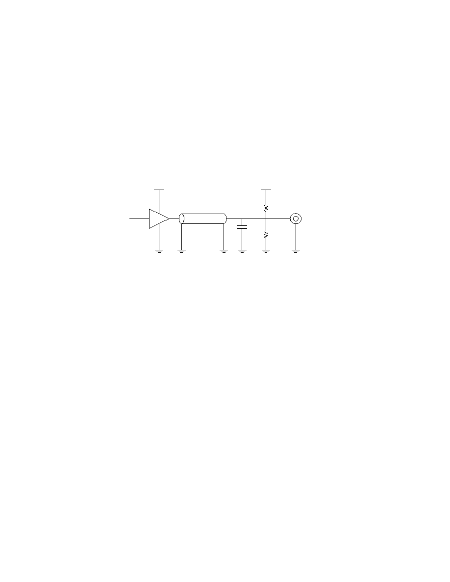
VDD
DUT
Zo = 50-ohms
VDD
CL = 40pF
RTERM
100-ohms
Test
Point
RTERM
100-ohms
Equivalent Test Load Circuit
相關(guān)PDF資料 |
PDF描述 |
|---|---|
| 5962F0253401VXC | 2.5 V FIXED POSITIVE REGULATOR, CDFP16 |
| L491333DIE2V | 3.3 V FIXED POSITIVE REGULATOR, UUC |
| 5962F9654403QXA | OTHER DECODER/DRIVER, CDFP16 |
| 5962F9657601QCX | AC SERIES, 4-BIT LOOK-AHEAD CARRY GENERATOR, TRUE OUTPUT, CDIP16 |
| 5962F9657701VXC | ACT SERIES, 4-BIT LOOK-AHEAD CARRY GENERATOR, TRUE OUTPUT, CDFP16 |
相關(guān)代理商/技術(shù)參數(shù) |
參數(shù)描述 |
|---|---|
| 5962D9563201VXC | 制造商:STMicroelectronics 功能描述:RS-432LINE DRIVERQUADFLAT16, GOLD - Bulk |
| 5962D9666301VXC | 制造商:STMicroelectronics 功能描述:RS-432LINE DRIVERQUADFLAT16, GOLD - Bulk |
| 5962F0052301QXC | 制造商:Intersil Corporation 功能描述: |
| 5962F0052301VXC | 制造商:Intersil Corporation 功能描述: |
| 5962F0151001VXC | 制造商:Intersil Corporation 功能描述:RAD SEU HARD QUAD COMPARATOR, CLASS V - Bulk |
發(fā)布緊急采購,3分鐘左右您將得到回復(fù)。