- 您現(xiàn)在的位置:買賣IC網(wǎng) > PDF目錄385949 > TSB81BA3I (Texas Instruments, Inc.) IEEE 1394b THREE-PORT CABLE TRANSCEIVER/ARBITER PDF資料下載
參數(shù)資料
| 型號: | TSB81BA3I |
| 廠商: | Texas Instruments, Inc. |
| 英文描述: | IEEE 1394b THREE-PORT CABLE TRANSCEIVER/ARBITER |
| 中文描述: | 的IEEE 1394b三端口電纜收發(fā)器/仲裁者 |
| 文件頁數(shù): | 10/57頁 |
| 文件大?。?/td> | 810K |
| 代理商: | TSB81BA3I |
第1頁第2頁第3頁第4頁第5頁第6頁第7頁第8頁第9頁當(dāng)前第10頁第11頁第12頁第13頁第14頁第15頁第16頁第17頁第18頁第19頁第20頁第21頁第22頁第23頁第24頁第25頁第26頁第27頁第28頁第29頁第30頁第31頁第32頁第33頁第34頁第35頁第36頁第37頁第38頁第39頁第40頁第41頁第42頁第43頁第44頁第45頁第46頁第47頁第48頁第49頁第50頁第51頁第52頁第53頁第54頁第55頁第56頁第57頁
SLLS559B DECEMBER 2002 REVISED OCTOBER 2003
10
POST OFFICE BOX 655303
DALLAS, TEXAS 75265
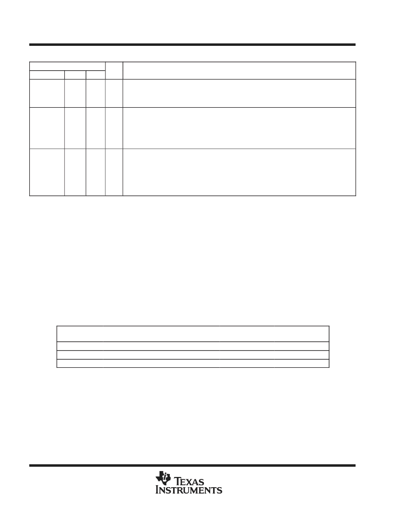
Terminal Functions (Continued)
TERMINAL
I/O
DESCRIPTION
NAME
TPA2
TPA2+
TPB2
TPB2+
TYPE
Cable
NO.
58
59
55
56
I/O
Port 2 twisted-pair differential-signal terminals. Board traces from each pair of positive and negative
differential signal terminals must be kept matched and as short as possible to the external load
resistors and to the cable connector. Please request the S800 1394b layout recommendations
document from your TI representative.
TPBIAS0
TPBIAS1
TPBIAS2
Cable
47
54
60
I/O
Twisted-pair bias output. This provides the 1.86-V nominal bias voltage needed for proper operation of
the twisted-pair cable drivers and receivers, and for signaling to the remote nodes that there is an active
cable connection in 1394a2000 mode. Each of these terminals, except for an unused port, must be
decoupled with a 1.0-
μ
F capacitor to ground. For the unused port, this terminal can be left
unconnected. Please request the S800 1394b layout recommendations document from your TI
representative.
XI
Osc In
27
Oscillator input. This terminal connects to a 98.304-MHz low jitter external oscillator. The XI terminal is
a 1.8-V CMOS input.
Oscillator jitter must be 5 ps RMS or better.
If only 3.3-V oscillators can be acquired, then great care must be taken to not introduce significant jitter
by the means used to level shift from 3.3 V to 1.8 V. If a resistor divider is used, then a high current
oscillator and low-value resistors must be used to minimize RC time constants. If a level-shifting circuit
is used, then it must introduce very little jitter. Please see layout recommendations document.
absolute maximum ratings over operating free-air temperature (unless otherwise noted)
Supply voltage range, V
DD
(see Note 1)
Input voltage range, V
I
(see Note 1)
Output voltage range at any output, V
O
Continuous total power dissipation
Operating free air temperature, T
A
: TSB81BA3
0.3 V to 4 V
. . . . . . . . . . . . . . . . . . . . . . . . . . . . . . . . . . . . . . . . . . . . . .
. . . . . . . . . . . . . . . . . . . . . . . . . . . . . . . . . . . . . . . . . . .
. . . . . . . . . . . . . . . . . . . . . . . . . . . . . . . . . . . . . . . .
. . . . . . . . . . . . . . . . . . . . . . . . . . . . . . . . . . . . .
. . . . . . . . . . . . . . . . . . . . . . . . . . . . . . . . . . . . . . . . .
TSB81BA3I
. . . . . . . . . . . . . . . . . . . . . . . . . . . . . . . . . . . . . .
. . . . . . . . . . . . . . . . . . . . . . . . . . . . . . . . . . . . . . . . . . . . . . . . . . .
0.5 V to V
DD
+ 0.5 V
0.5 V to V
DD
+ 0.5 V
See Dissipation Rating Table
0
°
C to 70
°
C
40
°
C to 85
°
C
65
°
C to 150
°
C
Storage temperature range, T
stg
Lead temperature 1,6 mm (1/16 inch) from case for 10 seconds
260
°
C
. . . . . . . . . . . . . . . . . . . . . . . . . . . . . . .
Stresses beyond those listed under “absolute maximum ratings” may cause permanent damage to the device. These are stress ratings only, and
functional operation of the device at these or any other conditions beyond those indicated under “recommended operating conditions” is not
implied. Exposure to absolute-maximum-rated conditions for extended periods may affect device reliability.
NOTE 1: All voltage values, except differential I/O bus voltages, are with respect to network ground.
DISSIPATION RATING TABLE
DERATING FACTOR
ABOVE TA = 25
°
C
52.5 mW/
°
C
31.7 mW/
°
C
20.3 mW/
°
C
PACKAGE
TA
≤
25
°
C
POWER RATING
TA = 70
°
C
POWER RATING
TA = 85
°
C
POWER RATING
PFP§
PFP
PFP#
5.05 W
2.69 W
1.9 W
3.05 W
1.62 W
1.15 W
2.01 W
1.1 W
792 mW
This is the inverse of the traditional junction-to-ambient thermal resistance (R
θ
JA).
§2 oz. trace and copper pad with solder.
2 oz. trace and copper pad without solder.
#For more information, refer to TI application note
PowerPAD
Thermally Enhanced Package,
(SLMA002).
PowerPAD is a trademark of Texas Instruments.
相關(guān)PDF資料 |
PDF描述 |
|---|---|
| TSE-0155-32S-P1-3 | SINGLE MODE SINGLE FIBER TRANSCEIVER |
| TSL230 | PROGRAMMABLE LIGHT-TO-FREQUENCY CONVERTERS |
| TSL235(中文) | Programmable Light-To-Frequency Converter(光頻轉(zhuǎn)換器) |
| TSL245(中文) | IR Light-To-Frequency Converter(紅外光頻轉(zhuǎn)換器) |
| TSL250(中文) | Light-To-Voltage Converter(光壓轉(zhuǎn)換器) |
相關(guān)代理商/技術(shù)參數(shù) |
參數(shù)描述 |
|---|---|
| TSB81BA3IPFP | 功能描述:射頻收發(fā)器 s800 3-Port Cable Xcvr/Arbiter RoHS:否 制造商:Atmel 頻率范圍:2322 MHz to 2527 MHz 最大數(shù)據(jù)速率:2000 Kbps 調(diào)制格式:OQPSK 輸出功率:4 dBm 類型: 工作電源電壓:1.8 V to 3.6 V 最大工作溫度:+ 85 C 接口類型:SPI 封裝 / 箱體:QFN-32 封裝:Tray |
| TSB81BA3IPFPEP | 功能描述:射頻收發(fā)器 Mil Enh 3-Port Cable Xcvr/Arbiter RoHS:否 制造商:Atmel 頻率范圍:2322 MHz to 2527 MHz 最大數(shù)據(jù)速率:2000 Kbps 調(diào)制格式:OQPSK 輸出功率:4 dBm 類型: 工作電源電壓:1.8 V to 3.6 V 最大工作溫度:+ 85 C 接口類型:SPI 封裝 / 箱體:QFN-32 封裝:Tray |
| TSB81BA3PFP | 功能描述:射頻收發(fā)器 s800 3-Port Cable Xcvr/Arbiter RoHS:否 制造商:Atmel 頻率范圍:2322 MHz to 2527 MHz 最大數(shù)據(jù)速率:2000 Kbps 調(diào)制格式:OQPSK 輸出功率:4 dBm 類型: 工作電源電壓:1.8 V to 3.6 V 最大工作溫度:+ 85 C 接口類型:SPI 封裝 / 箱體:QFN-32 封裝:Tray |
| TSB81BA3PFPG4 | 功能描述:射頻收發(fā)器 s800 3-Port Cable Xcvr/Arbiter RoHS:否 制造商:Atmel 頻率范圍:2322 MHz to 2527 MHz 最大數(shù)據(jù)速率:2000 Kbps 調(diào)制格式:OQPSK 輸出功率:4 dBm 類型: 工作電源電壓:1.8 V to 3.6 V 最大工作溫度:+ 85 C 接口類型:SPI 封裝 / 箱體:QFN-32 封裝:Tray |
| TSB82AA2 | 制造商:TI 制造商全稱:Texas Instruments 功能描述:1394b OHCI-LYNX CONTROLLER |
發(fā)布緊急采購,3分鐘左右您將得到回復(fù)。