- 您現(xiàn)在的位置:買賣IC網(wǎng) > PDF目錄371186 > TLIU04C1 (Lineage Power) Quad T1/E1 Line Interface(四T1/E1線接口) PDF資料下載
參數(shù)資料
| 型號(hào): | TLIU04C1 |
| 廠商: | Lineage Power |
| 英文描述: | Quad T1/E1 Line Interface(四T1/E1線接口) |
| 中文描述: | 四T1/E1線路接口(四個(gè)T1/E1線接口) |
| 文件頁(yè)數(shù): | 10/100頁(yè) |
| 文件大?。?/td> | 1321K |
| 代理商: | TLIU04C1 |
第1頁(yè)第2頁(yè)第3頁(yè)第4頁(yè)第5頁(yè)第6頁(yè)第7頁(yè)第8頁(yè)第9頁(yè)當(dāng)前第10頁(yè)第11頁(yè)第12頁(yè)第13頁(yè)第14頁(yè)第15頁(yè)第16頁(yè)第17頁(yè)第18頁(yè)第19頁(yè)第20頁(yè)第21頁(yè)第22頁(yè)第23頁(yè)第24頁(yè)第25頁(yè)第26頁(yè)第27頁(yè)第28頁(yè)第29頁(yè)第30頁(yè)第31頁(yè)第32頁(yè)第33頁(yè)第34頁(yè)第35頁(yè)第36頁(yè)第37頁(yè)第38頁(yè)第39頁(yè)第40頁(yè)第41頁(yè)第42頁(yè)第43頁(yè)第44頁(yè)第45頁(yè)第46頁(yè)第47頁(yè)第48頁(yè)第49頁(yè)第50頁(yè)第51頁(yè)第52頁(yè)第53頁(yè)第54頁(yè)第55頁(yè)第56頁(yè)第57頁(yè)第58頁(yè)第59頁(yè)第60頁(yè)第61頁(yè)第62頁(yè)第63頁(yè)第64頁(yè)第65頁(yè)第66頁(yè)第67頁(yè)第68頁(yè)第69頁(yè)第70頁(yè)第71頁(yè)第72頁(yè)第73頁(yè)第74頁(yè)第75頁(yè)第76頁(yè)第77頁(yè)第78頁(yè)第79頁(yè)第80頁(yè)第81頁(yè)第82頁(yè)第83頁(yè)第84頁(yè)第85頁(yè)第86頁(yè)第87頁(yè)第88頁(yè)第89頁(yè)第90頁(yè)第91頁(yè)第92頁(yè)第93頁(yè)第94頁(yè)第95頁(yè)第96頁(yè)第97頁(yè)第98頁(yè)第99頁(yè)第100頁(yè)
Advance Data Sheet, Rev. 2
TLIU04C1 Quad T1/E1 Line Interface
April 1999
10
Lucent Technologies Inc.
Microprocessor Mode
(continued)
Pin Information
(continued)
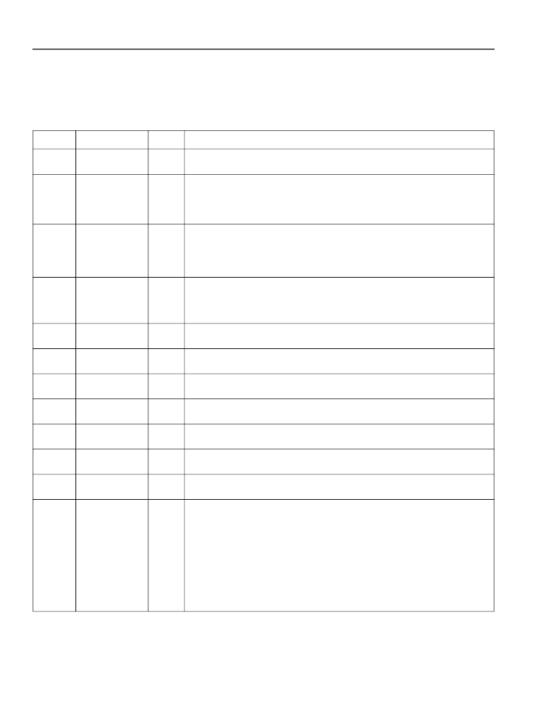
Table 1. Pin Descriptions
* I = input, O = output, I
u
indicates an input with internal pull-up; I
d
indicates an input with internal pull-down, P = power. Resistance value of all
internal pull-ups or pull-downs is 50 k
, unless otherwise specified.
Pin
Symbol
Type
*
I
d
Name/Description
117
CLKS
XCLK Select.
This pin selects either a 16x rate clock for XCLK (CLKS = 0)
or a primary line rate clock for XCLK (CLKS = 1).
XCLK Mode.
This pin must be set appropriately when using a primary line
rate clock for XCLK.
CEPT:
CLKM = 1.
DS1:
CLKM = 0.
Chip Mode.
This pin sets the chip mode for either direct logic mode or
microprocessor mode.
116
CLKM
I
d
118
CMODE
I
d
Microprocessor: CMODE = 1.
Direct Logic: CMODE = 0.
Ground Reference for Line Drivers.
128, 132
25, 29,
56, 60,
97, 101
129, 28,
57, 100
130, 27,
58, 99
131, 26,
59, 98
133, 24,
61, 96
134, 23,
62, 95
135, 22,
63, 94
136, 21,
64, 93
137, 20,
65, 92
GND
X
[1—4]
P
TTIP[1—4]
O
Transmit Bipolar Tip.
Positive bipolar transmit data to the analog line
interface.
Power Supply for Line Drivers.
The TLIU04C1 device requires a 5 V ± 5%
power supply on these pins.
Transmit Bipolar Ring.
Negative bipolar transmit data to the analog line
interface.
Power Supply for Analog Circuitry.
The TLIU04C1 device requires a 5 V
± 5% power supply on these pins.
Receive Bipolar Tip.
Positive bipolar receive data from the analog line
interface.
Receive Bipolar Ring.
Negative bipolar receive data from the analog line
interface.
Ground Reference for Analog Circuitry.
V
DDX
[1—4]
P
TRING[1—4]
O
V
DDA
[1—4]
P
RTIP[1—4]
I
RRING[1—4]
I
GND
A
[1—4]
P
RND/BPV[1—4]
O
Receive Negative Data.
When in dual-rail (DUAL = 1: register 5, bit 4)
clock recovery mode (CDR = 1: register 5, bit 0), this signal is the received
negative NRZ data to the terminal equipment. When in data slicing mode
(CDR = 0), this signal is the raw sliced negative data of the front end.
Bipolar Violation.
When in single-rail (DUAL = 0: register 5, bit 4) clock
recovery mode (CDR = 1: register 5, bit 0), and CODE = 1 (register 5, bit 3),
this signal is asserted high to indicate the occurrence of a code violation in
the receive data stream. A code violation is a bipolar violation that is not
part of a zero substitution code. If CODE = 0, this signal is asserted to
indicate the occurrence of a bipolar violation in the received data.
相關(guān)PDF資料 |
PDF描述 |
|---|---|
| TLV3011AIDBVR | Nanopower, 1.8V, SOT23 Comparator with Voltage Reference |
| TLV349x | CAPACITOR, CLASS Y2 1.0NFCAPACITOR, CLASS Y2 1.0NF; Capacitance:1nF; Voltage rating, AC:250V; Voltage rating, DC:2500V; Capacitor dielectric type:Polypropylene; Series:B81122; Tolerance, +:20%; Tolerance, -:20%; Temp, op. |
| TLV3011AIDBVT | Nanopower, 1.8V, SOT23 Comparator with Voltage Reference |
| TLV3011AIDCKR | Nanopower, 1.8V, SOT23 Comparator with Voltage Reference |
| TLV3011AIDCKT | Nanopower, 1.8V, SOT23 Comparator with Voltage Reference |
相關(guān)代理商/技術(shù)參數(shù) |
參數(shù)描述 |
|---|---|
| TLIXF30001 | 制造商:GIGA 功能描述: |
| TLIXF30003 | 制造商:Rochester Electronics LLC 功能描述:- Bulk |
| TLIXF30007-852838 | 制造商:Cortina Systems Inc 功能描述: |
| TLIXF30009-865852 | 功能描述:IC OPT TRANSPORT PROC 868-TBGA RoHS:是 類別:集成電路 (IC) >> 接口 - 電信 系列:- 產(chǎn)品培訓(xùn)模塊:Lead (SnPb) Finish for COTS 產(chǎn)品變化通告:Product Discontinuation 06/Feb/2012 標(biāo)準(zhǔn)包裝:750 系列:* |
| TLIXF30010 | 制造商:Intel 功能描述: |
發(fā)布緊急采購(gòu),3分鐘左右您將得到回復(fù)。