- 您現在的位置:買賣IC網 > PDF目錄370782 > HYB18T256324F-20 (INFINEON TECHNOLOGIES AG) 256-Mbit GDDR3 DRAM [600MHz] PDF資料下載
參數資料
| 型號: | HYB18T256324F-20 |
| 廠商: | INFINEON TECHNOLOGIES AG |
| 英文描述: | 256-Mbit GDDR3 DRAM [600MHz] |
| 中文描述: | 256兆GDDR3顯示內存[600MHz的] |
| 文件頁數: | 47/80頁 |
| 文件大小: | 2026K |
| 代理商: | HYB18T256324F-20 |
第1頁第2頁第3頁第4頁第5頁第6頁第7頁第8頁第9頁第10頁第11頁第12頁第13頁第14頁第15頁第16頁第17頁第18頁第19頁第20頁第21頁第22頁第23頁第24頁第25頁第26頁第27頁第28頁第29頁第30頁第31頁第32頁第33頁第34頁第35頁第36頁第37頁第38頁第39頁第40頁第41頁第42頁第43頁第44頁第45頁第46頁當前第47頁第48頁第49頁第50頁第51頁第52頁第53頁第54頁第55頁第56頁第57頁第58頁第59頁第60頁第61頁第62頁第63頁第64頁第65頁第66頁第67頁第68頁第69頁第70頁第71頁第72頁第73頁第74頁第75頁第76頁第77頁第78頁第79頁第80頁
HYB18T256324F–[16/20/22]
256-Mbit DDR SGRAM
Functional Description
Data Sheet
47
Rev. 1.11, 04-2005
10292004-DOXT-FS0U
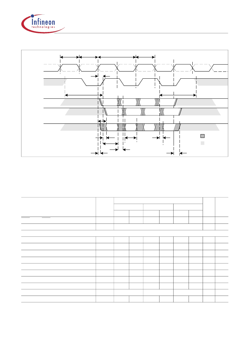
Figure 30
Basic Read Burst Timing
1. The GDDR3 SGRAM switches off the DQ terminations one cycle before data appears on the busand drives
the data bus HIGH.
2. The GDDR3 SGRAM drives the data bus HIGH one cycle after the last data driven on the bus before switching
the termination on again.
1.
t
CCD
is either for gapless consecutive reads or gapless consecutive writes.
2. Please round up
t
RTW
to the next integer of
t
CK
.
3.
t
HP
is the minimum of
t
CL
and
t
CH
4. Timing parameters defined with controller terminations on.
Table 25
Parameter
READ Timing Parameters for –1.6, –2.0 and –2.2 speed sorts
Symbol
Limit Values
–2.0
min
2
Unit
Note
–1.6
–2.2
min
2
max
—
max
—
min
2
max
—
CAS (a) to CAS (b) Command period
t
CCD
t
RTW
t
CK
t
CK
1
2
Read to Write command delay
Read Cycle Timing Parameters for Data and Data Strobe
Data Access Time from Clock
Read Preamble
t
RTW
(min)= (CL+4-WL)
t
AC
t
RPRE
t
RPST
–0.4
0.75
0.4
1.25
–0.4
0.75
0.4
1.25
–0.45
0.75
0.45
1.25
ns
t
CK
t
CK
4
Read Postamble
Data-out high impedance time from CLK
t
HZ
Data-out low impedance time from CLK
t
LZ
RDQS edge to Clock edge skew
RDQS edge to output data edge skew
Data hold skew factor
Data output hold time from RDQS
Minimum clock half period
0.75
t
ACmin
t
ACmin
–0.4
—
0
t
HP
–
t
QHS
0.45
1.25
t
ACmax
t
ACmin
t
ACmax
t
ACmin
0.4
0.225 —
0.225 0
0.75
1.25
t
ACmax
t
ACmin
t
ACmax
t
ACmin
0.4
0.225 —
0.225 0
0.75
1.25
t
ACmax
n
s
t
ACmax
n
s
0.45
0.25
0.25
4
4
4
4
4
4
3
t
DQSCK
t
DQSQ
t
QHS
t
QH
t
HP
–0.4
–0.45
ns
ns
ns
ns
t
CK
t
HP
–
t
QHS
0.45
t
HP
–
t
QHS
0.45
—
—
—
T
2034
2$13
$ONgT #ARE
!LL $1S COLLECTIVELY
#,+
#,+
T
#(
T
#,
T
1(
T
$1 31
T
$13#+
T
!#
T
202%
T
#+
T
(0
T
$1 31
T
1(3
$1 FIRST DATA VALID
$1 LAST DATA VALID
$
$
$
$
DATA
VALID
WINDOW
T
,:
T
(:
$
$
$
$
$
$
$
$
(I : .OT DRIVEN
BY $$2))) 3'2!-
0REAMBLE
0OSTAMBLE
相關PDF資料 |
PDF描述 |
|---|---|
| HYB18T256324F-22 | 256-Mbit GDDR3 DRAM [600MHz] |
| HYB18T256400AFL-3 | 256 Mbi t DDR2 SDRAM |
| HYB18T256160A-3S | 256 Mbi t DDR2 SDRAM |
| HYB18T256800AFL-3 | 256 Mbi t DDR2 SDRAM |
| HYB18T256400AFL-37 | 256 Mbi t DDR2 SDRAM |
相關代理商/技術參數 |
參數描述 |
|---|---|
| HYB18T256400AF-3.7 | 制造商:Infineon Technologies AG 功能描述:64M X 4 DDR DRAM, 0.5 ns, PBGA60 |
| HYB18T256400AF-5 | 制造商:Infineon Technologies AG 功能描述:SDRAM, DDR, 64M x 4, 60 Pin, Plastic, BGA |
| HYB18T256800AF-5 | 制造商:Infineon Technologies AG 功能描述: |
| HYB18T512161BF-25 | 制造商:Qimonda 功能描述:SDRAM, DDR, 32M x 16, 84 Pin, Plastic, BGA |
| HYB18T512400AF-5 | 制造商:Intersil Corporation 功能描述:SDRAM, DDR, 128M x 4, 60 Pin, Plastic, BGA |
發(fā)布緊急采購,3分鐘左右您將得到回復。