- 您現(xiàn)在的位置:買賣IC網(wǎng) > PDF目錄69010 > M30835MJGP 32-BIT, MROM, 30 MHz, MICROCONTROLLER, PQFP144 PDF資料下載
參數(shù)資料
| 型號: | M30835MJGP |
| 元件分類: | 微控制器/微處理器 |
| 英文描述: | 32-BIT, MROM, 30 MHz, MICROCONTROLLER, PQFP144 |
| 封裝: | PLASTIC, QFP-144 |
| 文件頁數(shù): | 259/441頁 |
| 文件大小: | 3861K |
| 代理商: | M30835MJGP |
第1頁第2頁第3頁第4頁第5頁第6頁第7頁第8頁第9頁第10頁第11頁第12頁第13頁第14頁第15頁第16頁第17頁第18頁第19頁第20頁第21頁第22頁第23頁第24頁第25頁第26頁第27頁第28頁第29頁第30頁第31頁第32頁第33頁第34頁第35頁第36頁第37頁第38頁第39頁第40頁第41頁第42頁第43頁第44頁第45頁第46頁第47頁第48頁第49頁第50頁第51頁第52頁第53頁第54頁第55頁第56頁第57頁第58頁第59頁第60頁第61頁第62頁第63頁第64頁第65頁第66頁第67頁第68頁第69頁第70頁第71頁第72頁第73頁第74頁第75頁第76頁第77頁第78頁第79頁第80頁第81頁第82頁第83頁第84頁第85頁第86頁第87頁第88頁第89頁第90頁第91頁第92頁第93頁第94頁第95頁第96頁第97頁第98頁第99頁第100頁第101頁第102頁第103頁第104頁第105頁第106頁第107頁第108頁第109頁第110頁第111頁第112頁第113頁第114頁第115頁第116頁第117頁第118頁第119頁第120頁第121頁第122頁第123頁第124頁第125頁第126頁第127頁第128頁第129頁第130頁第131頁第132頁第133頁第134頁第135頁第136頁第137頁第138頁第139頁第140頁第141頁第142頁第143頁第144頁第145頁第146頁第147頁第148頁第149頁第150頁第151頁第152頁第153頁第154頁第155頁第156頁第157頁第158頁第159頁第160頁第161頁第162頁第163頁第164頁第165頁第166頁第167頁第168頁第169頁第170頁第171頁第172頁第173頁第174頁第175頁第176頁第177頁第178頁第179頁第180頁第181頁第182頁第183頁第184頁第185頁第186頁第187頁第188頁第189頁第190頁第191頁第192頁第193頁第194頁第195頁第196頁第197頁第198頁第199頁第200頁第201頁第202頁第203頁第204頁第205頁第206頁第207頁第208頁第209頁第210頁第211頁第212頁第213頁第214頁第215頁第216頁第217頁第218頁第219頁第220頁第221頁第222頁第223頁第224頁第225頁第226頁第227頁第228頁第229頁第230頁第231頁第232頁第233頁第234頁第235頁第236頁第237頁第238頁第239頁第240頁第241頁第242頁第243頁第244頁第245頁第246頁第247頁第248頁第249頁第250頁第251頁第252頁第253頁第254頁第255頁第256頁第257頁第258頁當(dāng)前第259頁第260頁第261頁第262頁第263頁第264頁第265頁第266頁第267頁第268頁第269頁第270頁第271頁第272頁第273頁第274頁第275頁第276頁第277頁第278頁第279頁第280頁第281頁第282頁第283頁第284頁第285頁第286頁第287頁第288頁第289頁第290頁第291頁第292頁第293頁第294頁第295頁第296頁第297頁第298頁第299頁第300頁第301頁第302頁第303頁第304頁第305頁第306頁第307頁第308頁第309頁第310頁第311頁第312頁第313頁第314頁第315頁第316頁第317頁第318頁第319頁第320頁第321頁第322頁第323頁第324頁第325頁第326頁第327頁第328頁第329頁第330頁第331頁第332頁第333頁第334頁第335頁第336頁第337頁第338頁第339頁第340頁第341頁第342頁第343頁第344頁第345頁第346頁第347頁第348頁第349頁第350頁第351頁第352頁第353頁第354頁第355頁第356頁第357頁第358頁第359頁第360頁第361頁第362頁第363頁第364頁第365頁第366頁第367頁第368頁第369頁第370頁第371頁第372頁第373頁第374頁第375頁第376頁第377頁第378頁第379頁第380頁第381頁第382頁第383頁第384頁第385頁第386頁第387頁第388頁第389頁第390頁第391頁第392頁第393頁第394頁第395頁第396頁第397頁第398頁第399頁第400頁第401頁第402頁第403頁第404頁第405頁第406頁第407頁第408頁第409頁第410頁第411頁第412頁第413頁第414頁第415頁第416頁第417頁第418頁第419頁第420頁第421頁第422頁第423頁第424頁第425頁第426頁第427頁第428頁第429頁第430頁第431頁第432頁第433頁第434頁第435頁第436頁第437頁第438頁第439頁第440頁第441頁
Under
development
Preliminary Specifications REV.B3
Specifications in this manual are tentative and subject to change.
Mitsubishi Microcomputers
M32C/83 group
SINGLE-CHIP 16/32-BIT CMOS MICROCOMPUTER
Programmable I/O Port
330
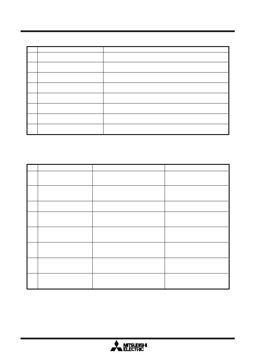
Table 1.29.3. Port P6 output control
PS0 register
PSL0 register
Bit 0 0: P60
Must set to "0"
________
1: UART0 output (RTS0)(Note)
Bit 1 0: P61
Must set to "0"
1: UART0 output (CLK0)(Note)
Bit 2 0: P62
0: UART0 output (SCL0)
1: Selected by PSL0 register
1: UART0 output (STxD0)
Bit 3 0: P63
Must set to "0"
1: UART0 output (TxD0/SDA0)(Note)
Bit 4 0: P64
________
0: UART1 output (RTS1)
1: Selected by PSL0 register
1: Intelligent I/O group 2 (OUTC21/ISCLK2)
Bit 5 0: P65
Must set to "0"
1: UART1 output (CLK1)(Note)
Bit 6 0: P66
0: UART1 output (SCL1)
1: Selected by PSL0 register
1: UART1 output (STxD1)
Bit 7 0: P67
Must set to "0"
1: UART1 output (TxD1/SDA1)(Note)
PS0 register: Function select register A0
PSL0 register: Function select register B0
Note : Select "0" in corresponding bit of PSL0 register.
Table 1.29.4. Port P7 output control
PS1 register
PSL1 register
PSC register
Bit 0 0: P70
0: Selected by PSC register
0: UART2 output (TxD2/SDA2)
1: Selected by PSL1 register
1: TImer output (TA0OUT)(Note 1)
1: Intelligent I/O group 2
(OUTC20/ISTxD2/IEOUT)
Bit 1 0: P71
0: Selected by PSC register
0: UART2 output (SCL2)
1: Selected by PSL1 register
1: UART2 output (STxD2)(Note 1)
1: Intelligent I/O group 2
(OUTC22)
Bit 2 0: P72
0: Selected by PSC register
0: UART2 output (CLK2)
1: Selected by PSL1 register
1: TImer output (TA1OUT)(Note 1)
1: Three-phase PWM output (V)
Bit 3 0: P73
0: Selected by PSC register
_______
0: UART2 output (RTS2)
1: Selected by PSL1 register
__
1: Three-phase PWM output (V)(Note 1)
1: Intelligent I/O group 1
(OUTC10/ISTxD1/BE1OUT)
Bit 4 0: P74
0: Selected by PSC register
0: TImer output (TA2OUT)
1: Selected by PSL1 register
1: Three-phase PWM output (W)(Note 1)
1: Intelligent I/O group 1
(OUTC11/ISCLK1)
Bit 5 0: P75
___
0: Three-phase PWM output (W)(Note 1)
Must set to "0"
1: Selected by PSL1 register
1: Intelligent I/O group 1
(OUTC12)
Bit 6 0: P76
0: Selected by PSC register
0: Intelligent I/O group 0
(OUTC00/ISTxD0/BE0OUT)
1: Selected by PSL1 register
1: TImer output (TA3OUT)
1: CAN output (CANOUT)
Bit 7 0: P77
Must set to "0"
0: Key input interrupt signal enabled
1: Intelligent I/O group 0
1: Key input interrupt signal disabled
(OUTC01/ISCLK0)
PS1 register: Function select register A1
PSL1 register: Function select register B1
PSC register: Function select register C
Note 1: Select "0" in corresponding bit of PSC register.
Note 2: Select "0" in corresponding bit of PSL1 register.
相關(guān)PDF資料 |
PDF描述 |
|---|---|
| M30865FJGP | 32-BIT, FLASH, 32 MHz, MICROCONTROLLER, PQFP144 |
| M30865FJTGP | 32-BIT, FLASH, 32 MHz, MICROCONTROLLER, PQFP144 |
| M30865FJTGP | 32-BIT, FLASH, 32 MHz, MICROCONTROLLER, PQFP144 |
| M30873FHBGP-U3 | 32-BIT, FLASH, 32 MHz, MICROCONTROLLER, PQFP100 |
| M30873FHBGP#U3 | 32-BIT, FLASH, 32 MHz, MICROCONTROLLER, PQFP100 |
相關(guān)代理商/技術(shù)參數(shù) |
參數(shù)描述 |
|---|---|
| M30840MCT-XXXGP | 制造商:RENESAS 制造商全稱:Renesas Technology Corp 功能描述:SINGLE-CHIP 16/32-BIT CMOS MICROCOMPUTER |
| M30840MC-XXXFP | 制造商:RENESAS 制造商全稱:Renesas Technology Corp 功能描述:SINGLE-CHIP 16/32-BIT CMOS MICROCOMPUTER |
| M30840MC-XXXGP | 制造商:RENESAS 制造商全稱:Renesas Technology Corp 功能描述:SINGLE-CHIP 16/32-BIT CMOS MICROCOMPUTER |
| M30840ME-XXXFP | 制造商:RENESAS 制造商全稱:Renesas Technology Corp 功能描述:SINGLE-CHIP 16/32-BIT CMOS MICROCOMPUTER |
| M30840ME-XXXGP | 制造商:RENESAS 制造商全稱:Renesas Technology Corp 功能描述:SINGLE-CHIP 16/32-BIT CMOS MICROCOMPUTER |
發(fā)布緊急采購,3分鐘左右您將得到回復(fù)。