- 您現(xiàn)在的位置:買賣IC網(wǎng) > PDF目錄67684 > IBM25PPC970FX6UB267ET 64-BIT, 1800 MHz, RISC PROCESSOR, CBGA576 PDF資料下載
參數(shù)資料
| 型號(hào): | IBM25PPC970FX6UB267ET |
| 元件分類: | 微控制器/微處理器 |
| 英文描述: | 64-BIT, 1800 MHz, RISC PROCESSOR, CBGA576 |
| 封裝: | 25 X 25 MM, 1 MM PITCH, CERAMIC, BGA-576 |
| 文件頁數(shù): | 69/78頁 |
| 文件大?。?/td> | 3524K |
| 代理商: | IBM25PPC970FX6UB267ET |
第1頁第2頁第3頁第4頁第5頁第6頁第7頁第8頁第9頁第10頁第11頁第12頁第13頁第14頁第15頁第16頁第17頁第18頁第19頁第20頁第21頁第22頁第23頁第24頁第25頁第26頁第27頁第28頁第29頁第30頁第31頁第32頁第33頁第34頁第35頁第36頁第37頁第38頁第39頁第40頁第41頁第42頁第43頁第44頁第45頁第46頁第47頁第48頁第49頁第50頁第51頁第52頁第53頁第54頁第55頁第56頁第57頁第58頁第59頁第60頁第61頁第62頁第63頁第64頁第65頁第66頁第67頁第68頁當(dāng)前第69頁第70頁第71頁第72頁第73頁第74頁第75頁第76頁第77頁第78頁
Datasheet
PowerPC 970FX RISC Microprocessor
Version 2.5
March 26, 2007
System Design Information
Page 71 of 78
5.7 Input-Output Use
This section provides information about the PowerPC 970FX input and output signals and their use.
5.7.1 Chip Signal I/O and Test Pins
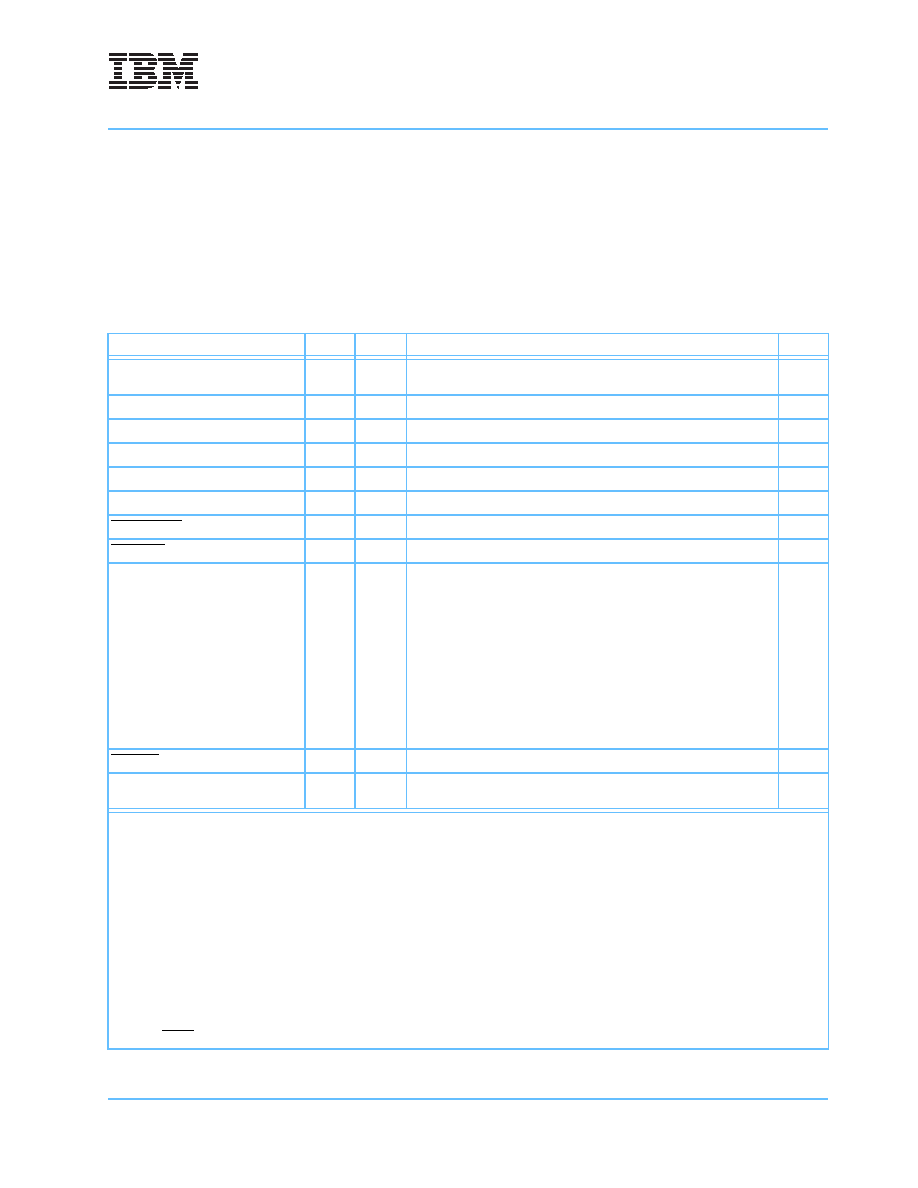
Table 5-8 shows the system signal names, debug, and test pins. There are 172 total chip pads. These
include three power/capacitance pins.
Table 5-8. Input/Output Signal Descriptions (Page 1 of 4)
Pin Name
Width
In/Out
System/Debug Function
Notes
ADIN(0:43)
44
In
System: Processor interface (PI) address or data and control informa-
tion.
—
ADOUT(0:43)
44
Out
System: PI address or data and control information out.
—
AFN
1
Out
Pin AFN is a spare output pin.
ANALOG_GND
1
Analog ground.
—
ATTENTION
1
Out
Debug: signal from PowerPC 970FX.
—
AVDD
1
In
Analog power supply.
—
AVP_RESET
1
In
For manufacturing test use only.
BI_MODE
1
In
Dedicated manufacturing signal.
BUS_CFG(0:2)
3
In
Bus configuration select. These signals select the bus frequency divi-
sion ratio from the processor clock to the bus speed.
‘000’
2:1
‘001’
3:1
‘010’
4:1
‘011’
6:1
‘100’
8:1
‘101’
12:1
‘110’
16:1
‘111’
Not valid
BYPASS
1
In
This signal is used to bypass the PLL.
C1_UND_GLOBAL
1
In
Debug: adjusts the C1 clock to internal latches and is not used for
normal operation.
Notes:
1. These are test signals for factory use only and must be pulled up to OVDD for normal processor operation.
2. For I2C or JTAG operation, the TCK and TDI signals must be pulled down to ground with a 10 k
Ω resistor. See Section 3.10.3 on
3. Bus ratios 8:1 and 16:1 are not supported for PI Input functionality.
4. These are test signals for factory use only and must be pulled down to GND for normal processor operation.
5. This signal should not be connected.
6. These pins can be used to measure on-chip voltage drop and noise. They should be connected to a backside probe point
immediately behind the module. They should not be connected to GND and VDD planes.
7. BiDi = bidirectional. OD = open drain.
8. Using the 4:1 or 12:1 ratio with multiplier of 12 limits the use of power tuning to (frequency)/2.
9. The PLL_MULT and PLL_RANGE(1:0) bits can be overwritten by JTAG commands and the BUS_CFG bits can be changed by
SCOM commands during the POR sequence. See the PowerPC 970FX Power On Reset Application Note for more details
10. Must be pulled down with a 10 k
Ω resistor to GND.
11. The TRST signal must be pulled up to OVDD with a 10 kΩ resistor.
相關(guān)PDF資料 |
PDF描述 |
|---|---|
| IBM25PPC970MP7TR21AFT | 64-BIT, 1600 MHz, RISC PROCESSOR, CBGA575 |
| IBM26BL486DX2-V66QP | 32-BIT, 66 MHz, MICROPROCESSOR, PQFP208 |
| IBM26BL486DX2-V80QP | 32-BIT, 80 MHz, MICROPROCESSOR, PQFP208 |
| IBM26BL486DX2-V50GP | 32-BIT, 50 MHz, MICROPROCESSOR, CPGA168 |
| IBM26BL486DX2-V50QP | 32-BIT, 50 MHz, MICROPROCESSOR, PQFP208 |
相關(guān)代理商/技術(shù)參數(shù) |
參數(shù)描述 |
|---|---|
| IBM25PPC970FX6UB429RT | 制造商:IBM Microelectronics 功能描述:MPU 970FX RISC 64BIT 90NM 1.5V 576CBGA - Trays 制造商:IBM 功能描述:IBM IBM25PPC970FX6UB429RT Co-Processors |
| IBM25PPC970GX7TR01-ET | 制造商:IBM 功能描述:ANTARES GX DD1.0X 1.2GHZ POWER OPTIMIZED - Trays |
| IBM25PPC970GX7TR05-ET | 制造商:IBM 功能描述:ANTARES GX DD1.0X 1.4GHZ POWER OPTIMIZED - Trays |
| IBM25PPC970GX7TR20-ET | 制造商:IBM Microelectronics 功能描述:ANTARES GX DD1.0X 1.6GHZ POWER OPTIMIZED - Trays |
| IBM25PPC970GX7TR23-ET | 制造商:IBM 功能描述:ANTARES GX DD1.0X 1.6GHZ PERFORMANCE OPTIMIZED - Trays |
發(fā)布緊急采購,3分鐘左右您將得到回復(fù)。