- 您現(xiàn)在的位置:買賣IC網(wǎng) > PDF目錄67684 > IBM25PPC970FX6UB267ET 64-BIT, 1800 MHz, RISC PROCESSOR, CBGA576 PDF資料下載
參數(shù)資料
| 型號(hào): | IBM25PPC970FX6UB267ET |
| 元件分類: | 微控制器/微處理器 |
| 英文描述: | 64-BIT, 1800 MHz, RISC PROCESSOR, CBGA576 |
| 封裝: | 25 X 25 MM, 1 MM PITCH, CERAMIC, BGA-576 |
| 文件頁數(shù): | 16/78頁 |
| 文件大小: | 3524K |
| 代理商: | IBM25PPC970FX6UB267ET |
第1頁第2頁第3頁第4頁第5頁第6頁第7頁第8頁第9頁第10頁第11頁第12頁第13頁第14頁第15頁當(dāng)前第16頁第17頁第18頁第19頁第20頁第21頁第22頁第23頁第24頁第25頁第26頁第27頁第28頁第29頁第30頁第31頁第32頁第33頁第34頁第35頁第36頁第37頁第38頁第39頁第40頁第41頁第42頁第43頁第44頁第45頁第46頁第47頁第48頁第49頁第50頁第51頁第52頁第53頁第54頁第55頁第56頁第57頁第58頁第59頁第60頁第61頁第62頁第63頁第64頁第65頁第66頁第67頁第68頁第69頁第70頁第71頁第72頁第73頁第74頁第75頁第76頁第77頁第78頁
Datasheet
PowerPC 970FX RISC Microprocessor
Version 2.5
March 26, 2007
Electrical and Thermal Characteristics
Page 23 of 78
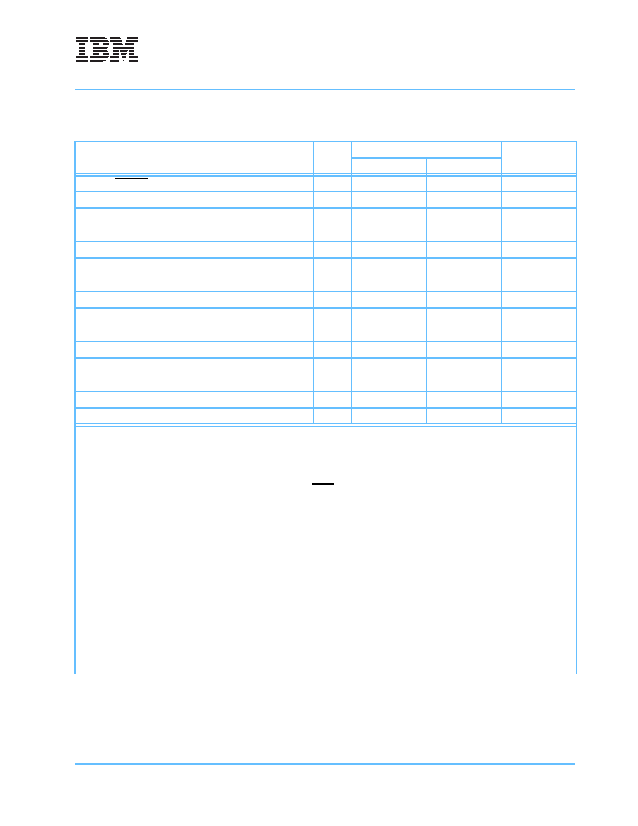
3.1.4 dc Electrical Specifications
Table 3-4. dc Electrical Specifications
Characteristic
Symbol
Voltage
Unit
Notes
Minimum
Maximum
SYSCLK, SYSCLK input high voltage
—
0.7
× OVDD
OVDD + 0.3
V
SYSCLK, SYSCLK input low voltage
—
-0.3
0.3
× OVDD
Processor interface (PI) input high voltage
VIH
(0.5
× OVDD) + 0.2
—
V
PI input low voltage
VIL
—
(0.5
× OVDD) - 0.2
V
NonPI input high voltage
VIH
0.7
× OVDD
—V
NonPI input low voltage
VIL
—0.3
× OVDD
PI output high voltage
VOH
0.78
× OVDD
—V
PI output low voltage
VOL
—
0.22
× OVDD
NonPI output high voltage, IOH = -2 mA
VOH
OVDD - 0.2
—
V
—
NonPI output low voltage, IOL = 2 mA
VOL
—0.2
V
—
Open drain (OD) output low, IOL = 2 mA (CHKSTOP, I2CGO)
VOL
—0.2
V
OD output low, IOL = 5 mA (I2C)
VOL
—0.2
V
Input leakage current, VIN = OVDD, VIN = 0 V
IIN
—60
μA—
Hi-Z (off state) leakage current, VOUT = OVDD, VOUT = 0 V
ITSO
—60
μA—
Input capacitance, VIN = 0 V, frequency = 1 MHz
CIN
—5.0
pF
Notes: See Table 3-2 on page 21 for recommended operating conditions.
1. SYSCLK differential receiver requires high-speed transceiver logic (HSTL) differential signaling level. See the Joint Electron Device
Engineering Council (JEDEC) HSTL standard.
2. See the electrical interface section of the PowerPC 970FX RISC Microprocessor Users Manual. The minimum input must meet the
signal eye opening requirements of the link.
3. The Joint Test Action Group (JTAG) signals TDI, TMS, and TRST do not have internal pullups; therefore, pullups must be added to
the system board. Pullups should be added and adjusted according to the system implementation. These input and outputs meet
the dc specification in the JEDEC standard JESD8-11 for 1.5 V normal power supply range.
4. A 100
Ω split terminator is the test load. Note that a 40 Ω signal driver has an up level of 0.78 × OVDD for VOH and 0.22 × OVDD at
VOL.
5. There are two open drain signals on this type of signal driver: CHKSTOP and I2CGO. The pullup for these nets depend on the Trise
time requirement, net load, and topology. The following examples are two bounding suggestions based on a point-to-point 50
Ω net
with two lengths (5 cm and 61 cm). A 33
Ω series source terminator was added in both runs. A net of 61 cm is recommended.
Examples:
500
Ω pullup dc low level 0.18 V at the receiver
Trise 0.2 V - 0.8 V = 55 ns at 61 cm
Trise 0.2 V - 0.8 V = 10 ns at 5 cm
1 k
Ω pullup dc low level 0.13 V at the receiver
Trise 0.2 V - 0.8 V = 115 ns at 61 cm
Trise 0.2 V - 0.8 V = 20 ns at 5 cm
6. Capacitance values are guaranteed by design and characterization, and are not tested.
相關(guān)PDF資料 |
PDF描述 |
|---|---|
| IBM25PPC970MP7TR21AFT | 64-BIT, 1600 MHz, RISC PROCESSOR, CBGA575 |
| IBM26BL486DX2-V66QP | 32-BIT, 66 MHz, MICROPROCESSOR, PQFP208 |
| IBM26BL486DX2-V80QP | 32-BIT, 80 MHz, MICROPROCESSOR, PQFP208 |
| IBM26BL486DX2-V50GP | 32-BIT, 50 MHz, MICROPROCESSOR, CPGA168 |
| IBM26BL486DX2-V50QP | 32-BIT, 50 MHz, MICROPROCESSOR, PQFP208 |
相關(guān)代理商/技術(shù)參數(shù) |
參數(shù)描述 |
|---|---|
| IBM25PPC970FX6UB429RT | 制造商:IBM Microelectronics 功能描述:MPU 970FX RISC 64BIT 90NM 1.5V 576CBGA - Trays 制造商:IBM 功能描述:IBM IBM25PPC970FX6UB429RT Co-Processors |
| IBM25PPC970GX7TR01-ET | 制造商:IBM 功能描述:ANTARES GX DD1.0X 1.2GHZ POWER OPTIMIZED - Trays |
| IBM25PPC970GX7TR05-ET | 制造商:IBM 功能描述:ANTARES GX DD1.0X 1.4GHZ POWER OPTIMIZED - Trays |
| IBM25PPC970GX7TR20-ET | 制造商:IBM Microelectronics 功能描述:ANTARES GX DD1.0X 1.6GHZ POWER OPTIMIZED - Trays |
| IBM25PPC970GX7TR23-ET | 制造商:IBM 功能描述:ANTARES GX DD1.0X 1.6GHZ PERFORMANCE OPTIMIZED - Trays |
發(fā)布緊急采購,3分鐘左右您將得到回復(fù)。