- 您現(xiàn)在的位置:買賣IC網(wǎng) > PDF目錄378216 > 82557 (Intel Corp.) Fast Ethernet PCI Bus Controller(快速以太網(wǎng) PCI總線控制器) PDF資料下載
參數(shù)資料
| 型號(hào): | 82557 |
| 廠商: | Intel Corp. |
| 英文描述: | Fast Ethernet PCI Bus Controller(快速以太網(wǎng) PCI總線控制器) |
| 中文描述: | 快速以太網(wǎng)PCI總線控制器(快速以太網(wǎng)的PCI總線控制器) |
| 文件頁數(shù): | 22/57頁 |
| 文件大?。?/td> | 601K |
| 代理商: | 82557 |
第1頁第2頁第3頁第4頁第5頁第6頁第7頁第8頁第9頁第10頁第11頁第12頁第13頁第14頁第15頁第16頁第17頁第18頁第19頁第20頁第21頁當(dāng)前第22頁第23頁第24頁第25頁第26頁第27頁第28頁第29頁第30頁第31頁第32頁第33頁第34頁第35頁第36頁第37頁第38頁第39頁第40頁第41頁第42頁第43頁第44頁第45頁第46頁第47頁第48頁第49頁第50頁第51頁第52頁第53頁第54頁第55頁第56頁第57頁
INTEL 82557 FAST ETHERNET PCI BUS CONTROLLER
22
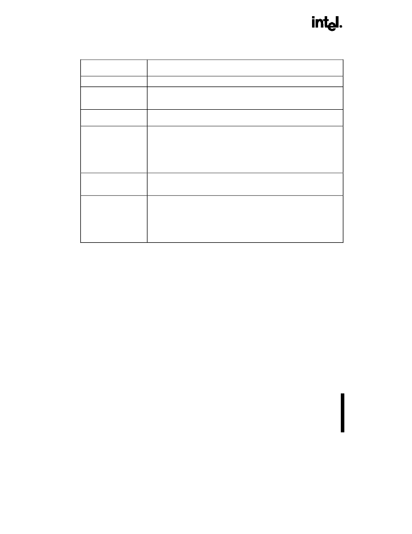
Table 5. Miscellaneous PCI Configuration Bits
Register
Description
Cache Line Size
This register is not implemented in the 82557. The value of this field is fixed to 0.
Latency Timer
The 82557, as a master device, implements this register to limit the size of very
long burst cycles. The initial value is 0 and is then programmed by system BIOS
at initialization time.
Built-in Self Test (BIST)
This optional register is used for control and status of BIST. The 82557 will not
provide PCI BIST and the value of this field is always set to 0.
Interrupt Line
The Interrupt Line register is an 8-bit register used to communicate interrupt line
routing information. This register is configurable in the 82557. POST software will
write the routing information into this register as it initializes and configures the
system. The value in this register defines which input of the system interrupt
controller(s) the device's interrupt pin is connected to. Device drivers and
operating systems can then use this information to determine priority and vector
information.
Interrupt Pin
The Interrupt Pin register tells which interrupt pin the device (or device function)
uses. This eight bit register is always set to a 1 in the 82557, indicating INTA# is
used.
MIN_GNT/ MAX_LAT
These read-only byte registers are used to specify the devices desired settings
for Latency Timer values. For both registers, the value specifies a period of time
specifying how often the device needs to gain access to the PCI bus. The values
microseconds) for MAX_LAT.
Base Address Registers
One of the most important functions for enabling
superior configurability and ease of use is the ability
to relocate PCI devices in the address spaces. At
system power-up device independent software must
be able to determine what devices are present, build
a consistent address map, and determine if a device
has an expansion ROM.
The 82557 contains three Base Address Registers
(BAR), two requesting memory mapped resources
and one requesting I/O mapping. Each register is 32-
bits wide. The least significant bit in BAR determines
whether it represents an I/O or memory space.
Figure 4 and Figure 5 show the layout of a BAR for
both I/O and memory mapping. After determining this
information, power-up software can map the I/O and
memory controllers into available locations and
proceed with system boot. In order to do this
mapping in a device independent manner, the base
registers for this mapping are placed in the
predefined header portion of configuration space.
Device drivers can then access this configuration
space to determine the mapping of a particular
device.
相關(guān)PDF資料 |
PDF描述 |
|---|---|
| 82559 | Fast Ethernet Multifunction PCI/CARD bus controller(快速以太網(wǎng)多功能PCI/CARD 總線控制器) |
| 8255A-5 | PROGRAMMABLE PERIPHEAL INTERFACE |
| 8255A | IC LOGIC 3257 4-BIT 1-OF-2 FET MULTIPLEXER/DEMULTIPLEXER -40+85C SSOP-16 - OBSOLETE |
| 8255A | Programmable Peripheral Interface iAPX86 Family |
| 8255A-5 | 12-Bit, 2.7 V to 5.25 V, 1.5 MSPS Low Power ADC; Package: SOIC - Wide; No of Pins: 24; Temperature Range: Industrial |
相關(guān)代理商/技術(shù)參數(shù) |
參數(shù)描述 |
|---|---|
| 8255702-025 | 制造商:ITT Interconnect Solutions 功能描述:NASA CONNECTOR - Bulk |
| 8255702-095 | 制造商:ITT Interconnect Solutions 功能描述:NASA CONNECTOR - Bulk |
| 8255702-096 | 制造商:ITT Interconnect Solutions 功能描述:NASA CONNECTOR - Bulk |
| 8255702-098 | 制造商:ITT Interconnect Solutions 功能描述:NASA CONNECTOR - Bulk |
| 8255704-050 | 制造商:ITT Interconnect Solutions 功能描述:NASA CONNECTOR - Bulk |
發(fā)布緊急采購,3分鐘左右您將得到回復(fù)。