- 您現(xiàn)在的位置:買賣IC網(wǎng) > PDF目錄382783 > μPD30102 (NEC Corp.) 64-/32-BIT Microprocessor(64/32位微處理器) PDF資料下載
參數(shù)資料
| 型號(hào): | μPD30102 |
| 廠商: | NEC Corp. |
| 英文描述: | 64-/32-BIT Microprocessor(64/32位微處理器) |
| 中文描述: | 64-/32-BIT微處理器(64/32位微處理器) |
| 文件頁數(shù): | 11/112頁 |
| 文件大?。?/td> | 639K |
| 代理商: | ΜPD30102 |
第1頁第2頁第3頁第4頁第5頁第6頁第7頁第8頁第9頁第10頁當(dāng)前第11頁第12頁第13頁第14頁第15頁第16頁第17頁第18頁第19頁第20頁第21頁第22頁第23頁第24頁第25頁第26頁第27頁第28頁第29頁第30頁第31頁第32頁第33頁第34頁第35頁第36頁第37頁第38頁第39頁第40頁第41頁第42頁第43頁第44頁第45頁第46頁第47頁第48頁第49頁第50頁第51頁第52頁第53頁第54頁第55頁第56頁第57頁第58頁第59頁第60頁第61頁第62頁第63頁第64頁第65頁第66頁第67頁第68頁第69頁第70頁第71頁第72頁第73頁第74頁第75頁第76頁第77頁第78頁第79頁第80頁第81頁第82頁第83頁第84頁第85頁第86頁第87頁第88頁第89頁第90頁第91頁第92頁第93頁第94頁第95頁第96頁第97頁第98頁第99頁第100頁第101頁第102頁第103頁第104頁第105頁第106頁第107頁第108頁第109頁第110頁第111頁第112頁
μ
PD30102
11
Preliminary Data Sheet
1. PIN FUNCTIONS
Remark
# indicates active low.
1.1 Pin Functions
(1) System bus interface signals
(1/2)
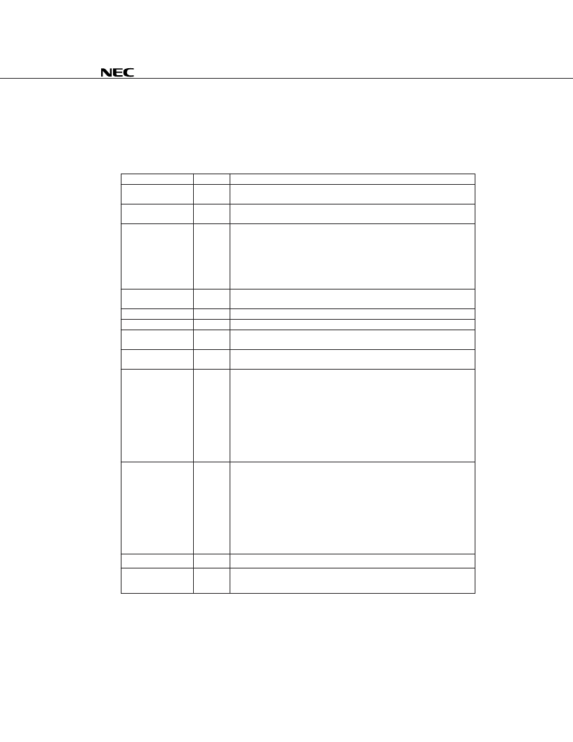
Signal Name
I/O
Function
ADD (0:25)
O
This is a 25-bit address bus. Used to specify addresses of the V
R
4102, DRAM, ROM,
LCD, and system bus (ISA).
DATA (0:15)
I/O
This is a 16-bit data bus. Used to transfer data from the V
R
4102 to DRAM, ROM, LCD,
and system bus, and vice versa.
DATA (16:31)/
GPIO (16:31)
I/O
This function differs depending on how the DBUS32 pin is set.
<When DBUS32 = 1>
It is the high-order 16 bits of the 32-bit data bus.
This bus is used for transmitting and receiving data between the V
R
4102 and the DRAM
and ROM.
<When DBUS32 = 0>
It is a general-purpose I/O (GPIO) port.
LCDCS#
O
This is the LCD chip select signal. This signal is active when the V
R
4102 is performing
LCD access using the ADD/DATA bus.
RD#
O
Active when the V
R
4102 is reading data from the LCD, RAM, or ROM.
WR#
O
Active when the V
R
4102 is writing data to the LCD, RAM, or ROM.
LCDRDY
I
This is the LCD ready signal. Set this signal as active when the LCD controller is ready
to be accessed from the V
R
4102.
ROMCS (0:3)#
O
This is the ROM chip select signal. It is used to select a ROM to be accessed from
among up to four connected ROM units.
UUCAS#/
MRAS3#
O
This function differs depending on how the DBUS32 pin is set.
<When DBUS32 = 1>
UUCAS#
This signal is active when a valid column address is output via the ADD bus during
access of DATA (24:31) in the 32-bit data bus.
<When DBUS32 = 0>
MRAS3#
This is the DRAM’s RAS signal. Up to four DRAM units can be connected, and this
signal is active when a valid row address is output via the ADD bus for the DRAM
connected to the high-order address.
ULCAS#/
MRAS2#
O
This function differs depending on how the DBUS32 pin is set.
<When DBUS32 = 1>
ULCAS#
This signal is active when a valid column address is output via the ADD bus during
access of DATA (16:23) in the 32-bit data bus.
<When DBUS32 = 0>
MRAS2#
This is the DRAM’s RAS signal. This signal is active when a valid row address is output
via the ADD bus for the DRAM connected to the next-highest address after the highest
high-order address.
MRAS (0:1)#
O
This is the DRAM’s RAS-only signal.
UCAS#
O
This is the DRAM’s CAS signal. This signal is active when a valid column address
is output via the ADD bus during access of DATA (8:15) in the DRAM.
相關(guān)PDF資料 |
PDF描述 |
|---|---|
| μPD30121 | 64-Bit MIPS RISC Microprocessor(64 位RISC 微處理器) |
| μPD30122 | 64-Bit RISC Microprosessor(64位RISC微處理器) |
| μPD30181 | 64-Bit RISC Microprosessor(64位RISC微處理器) |
| μPD30210 | 64-Bit MIPS RISC Microprocessor(64位MIPS RISC 微處理器) |
| μPD30200 | High-Performance, 64-Bit RISC Microprosessor(高性能64位RISC微處理器) |
相關(guān)代理商/技術(shù)參數(shù) |
參數(shù)描述 |
|---|---|
| PD301-024-03-PC | 制造商:未知廠家 制造商全稱:未知廠家 功能描述:Analog IC |
| PD301-024-03-P-C-200 | 制造商:未知廠家 制造商全稱:未知廠家 功能描述:DC to DC Converter |
| PD301-024-03-P-C-250 | 制造商:未知廠家 制造商全稱:未知廠家 功能描述:DC to DC Converter |
| PD301-024-03-P-C-300 | 制造商:未知廠家 制造商全稱:未知廠家 功能描述:DC to DC Converter |
| PD301-024-03-PI | 制造商:未知廠家 制造商全稱:未知廠家 功能描述:Analog IC |
發(fā)布緊急采購,3分鐘左右您將得到回復(fù)。