- 您現(xiàn)在的位置:買賣IC網(wǎng) > PDF目錄296800 > PEF22508E (INFINEON TECHNOLOGIES AG) DATACOM, PCM TRANSCEIVER, PBGA256 PDF資料下載
參數(shù)資料
| 型號: | PEF22508E |
| 廠商: | INFINEON TECHNOLOGIES AG |
| 元件分類: | 數(shù)字傳輸電路 |
| 英文描述: | DATACOM, PCM TRANSCEIVER, PBGA256 |
| 封裝: | 17 X 17 MM, 1 MM PITCH, PLASTIC, LBGA-256 |
| 文件頁數(shù): | 28/193頁 |
| 文件大?。?/td> | 10683K |
| 代理商: | PEF22508E |
第1頁第2頁第3頁第4頁第5頁第6頁第7頁第8頁第9頁第10頁第11頁第12頁第13頁第14頁第15頁第16頁第17頁第18頁第19頁第20頁第21頁第22頁第23頁第24頁第25頁第26頁第27頁當前第28頁第29頁第30頁第31頁第32頁第33頁第34頁第35頁第36頁第37頁第38頁第39頁第40頁第41頁第42頁第43頁第44頁第45頁第46頁第47頁第48頁第49頁第50頁第51頁第52頁第53頁第54頁第55頁第56頁第57頁第58頁第59頁第60頁第61頁第62頁第63頁第64頁第65頁第66頁第67頁第68頁第69頁第70頁第71頁第72頁第73頁第74頁第75頁第76頁第77頁第78頁第79頁第80頁第81頁第82頁第83頁第84頁第85頁第86頁第87頁第88頁第89頁第90頁第91頁第92頁第93頁第94頁第95頁第96頁第97頁第98頁第99頁第100頁第101頁第102頁第103頁第104頁第105頁第106頁第107頁第108頁第109頁第110頁第111頁第112頁第113頁第114頁第115頁第116頁第117頁第118頁第119頁第120頁第121頁第122頁第123頁第124頁第125頁第126頁第127頁第128頁第129頁第130頁第131頁第132頁第133頁第134頁第135頁第136頁第137頁第138頁第139頁第140頁第141頁第142頁第143頁第144頁第145頁第146頁第147頁第148頁第149頁第150頁第151頁第152頁第153頁第154頁第155頁第156頁第157頁第158頁第159頁第160頁第161頁第162頁第163頁第164頁第165頁第166頁第167頁第168頁第169頁第170頁第171頁第172頁第173頁第174頁第175頁第176頁第177頁第178頁第179頁第180頁第181頁第182頁第183頁第184頁第185頁第186頁第187頁第188頁第189頁第190頁第191頁第192頁第193頁
Data Sheet
123
Rev. 1.0, 2005-06-02
OctalLIUTM
PEF 22508 E
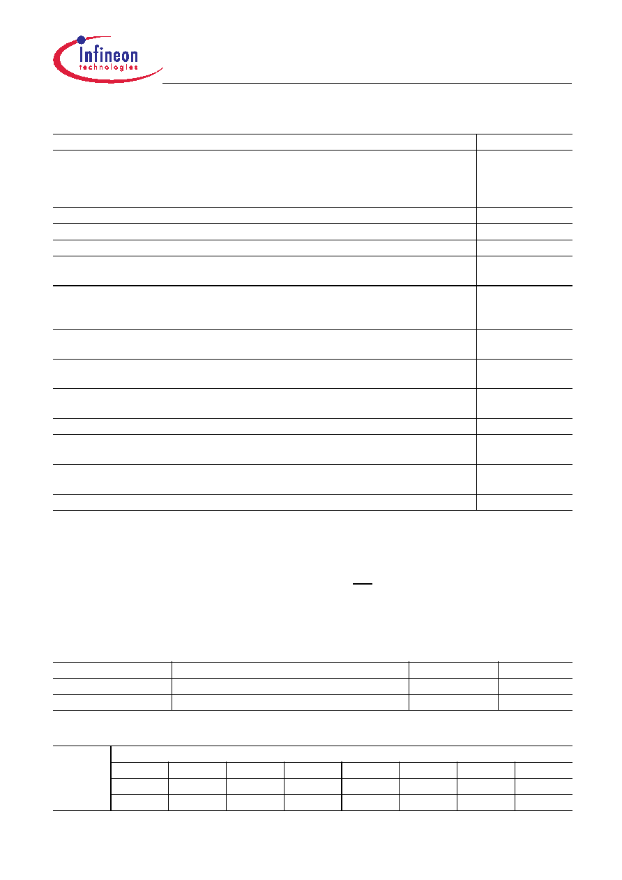
Register Description
Registers PC2 to PC3 have the same layout and description, but the 4 LSBs of PC3 are not used because only 2
MFPs in transmit direction exists.
The bits (3:0) of the register PC3 can be written and read, but are not valid.
Only one of the ports RPA, RPB or RPC must be configured as RTDMT.
Only one of the ports XPA or XPB must be configured as XLT or XLT.
The registers PC1, PC2 and PC4 have the reset values 00H, PC3 has the reset value F0H.
The Offset Addresses are listed in PCn Overview, for bit names refer to Port Configuration Registers.
TCLK: Transmit Clock (Input)
A 2.048/8.192 MHz clock has to be sourced by the system if the internal generated transmit
clock (DCO-X) is not used. Optionally this input is used as a synchronization clock for the
DCO-X circuitry with a frequency of 2.048 MHz.
0011B
reserved
0100B
reserved
0101B
reserved
0110B
XCLK: Transmit Line Clock (Output)
Frequency: 2.048 MHz
0111B
XLT: Transmit Line Tristate control input, high active
With a high level on this port the transmit lines XL1/2 or XDOP/N are set directly into tristate.
This pin function is logically ORd with register XPM2.XLT. See Chapter 3.9.1.
1000B
GPI: General Purpose Input, low level
Value of this input is stored in register MFPI.
1001B
GPOH: General Purpose Output, high level
Pin is set fixed to high level
1010B
GPOL: General Purpose Output, low level
Pin is set fixed to low level
1011B
reserved
1100B
XDIN: Transmit Data In Negative
Negative transmit data in for dual rail mode
1101B
XLT: Transmit Line Tristate control input, low active
see XLT
1110B
reserved
1111B
Table 43
PCn Overview
Register Short Name
Register Long Name
Offset Address
Page Number
PC2
Port Configuration Register 2
xx81H
PC3
Port Configuration Register 3
xx82H
Table 44
Port Configuration Registers
7
6
5
4
3
2
1
0
PC1
RPC13
RPC12
RPC11
RPC10
XPC13
XPC12
XPC11
XPC10
PC2
RPC23
RPC22
RPC21
RPC20
XPC23
XPC22
XPC21
XPC20
PC3
RPC33
RPC32
RPC31
RPC30
XPC33
XPC32
XPC31
XPC30
Table 42
XPC1 Constant Values (cont’d)
Name and Description
Value
相關PDF資料 |
PDF描述 |
|---|---|
| PEF22554E | DATACOM, FRAMER, PBGA160 |
| PEF22554HT | DATACOM, FRAMER, PQFP144 |
| PES12-42S-N0024 | |
| PESD3V3V4UK,132 | 25 W, UNIDIRECTIONAL, 4 ELEMENT, SILICON, TVS DIODE |
| PF38F3050L0YUQ3A | SPECIALTY MEMORY CIRCUIT, PBGA88 |
相關代理商/技術參數(shù) |
參數(shù)描述 |
|---|---|
| PEF22508EV1.1-G | 功能描述:網(wǎng)絡控制器與處理器 IC T/E RoHS:否 制造商:Micrel 產(chǎn)品:Controller Area Network (CAN) 收發(fā)器數(shù)量: 數(shù)據(jù)速率: 電源電流(最大值):595 mA 最大工作溫度:+ 85 C 安裝風格:SMD/SMT 封裝 / 箱體:PBGA-400 封裝:Tray |
| PEF22508EV11G | 制造商:Rochester Electronics LLC 功能描述: 制造商:Infineon Technologies AG 功能描述: |
| PEF22508EV11GXP | 制造商:Lantiq 功能描述:LINE INTERFACE UNITS |
| PEF22508EV11GXT | 制造商:Lantiq 功能描述:LINE INTERFACE UNITS |
| PEF22509EV1.1 | 制造商:Infineon Technologies AG 功能描述:SP000205605_T/E ASIC_TY_PB |
發(fā)布緊急采購,3分鐘左右您將得到回復。