- 您現(xiàn)在的位置:買賣IC網(wǎng) > PDF目錄377000 > DSP56321 (飛思卡爾半導(dǎo)體(中國(guó))有限公司) 24-Bit Digital Signal Processor PDF資料下載
參數(shù)資料
| 型號(hào): | DSP56321 |
| 廠商: | 飛思卡爾半導(dǎo)體(中國(guó))有限公司 |
| 元件分類: | 數(shù)字信號(hào)處理 |
| 英文描述: | 24-Bit Digital Signal Processor |
| 中文描述: | 24位數(shù)字信號(hào)處理器 |
| 文件頁(yè)數(shù): | 20/84頁(yè) |
| 文件大小: | 898K |
| 代理商: | DSP56321 |
第1頁(yè)第2頁(yè)第3頁(yè)第4頁(yè)第5頁(yè)第6頁(yè)第7頁(yè)第8頁(yè)第9頁(yè)第10頁(yè)第11頁(yè)第12頁(yè)第13頁(yè)第14頁(yè)第15頁(yè)第16頁(yè)第17頁(yè)第18頁(yè)第19頁(yè)當(dāng)前第20頁(yè)第21頁(yè)第22頁(yè)第23頁(yè)第24頁(yè)第25頁(yè)第26頁(yè)第27頁(yè)第28頁(yè)第29頁(yè)第30頁(yè)第31頁(yè)第32頁(yè)第33頁(yè)第34頁(yè)第35頁(yè)第36頁(yè)第37頁(yè)第38頁(yè)第39頁(yè)第40頁(yè)第41頁(yè)第42頁(yè)第43頁(yè)第44頁(yè)第45頁(yè)第46頁(yè)第47頁(yè)第48頁(yè)第49頁(yè)第50頁(yè)第51頁(yè)第52頁(yè)第53頁(yè)第54頁(yè)第55頁(yè)第56頁(yè)第57頁(yè)第58頁(yè)第59頁(yè)第60頁(yè)第61頁(yè)第62頁(yè)第63頁(yè)第64頁(yè)第65頁(yè)第66頁(yè)第67頁(yè)第68頁(yè)第69頁(yè)第70頁(yè)第71頁(yè)第72頁(yè)第73頁(yè)第74頁(yè)第75頁(yè)第76頁(yè)第77頁(yè)第78頁(yè)第79頁(yè)第80頁(yè)第81頁(yè)第82頁(yè)第83頁(yè)第84頁(yè)
DSP56321 Technical Data, Rev. 11
1-14
Freescale Semiconductor
Signals/Connections
1.11 JTAG and OnCE Interface
The DSP56300 family and in particular the DSP56321 support circuit-board test strategies based on the
IEEE
Std.
1149.1 test access port and boundary scan architecture, the industry standard developed under the
sponsorship of the Test Technology Committee of IEEE and the JTAG. The OnCE module provides a means to
interface nonintrusively with the DSP56300 core and its peripherals so that you can examine registers, memory, or
on-chip peripherals. Functions of the OnCE module are provided through the JTAG TAP signals. For programming
models, see the chapter on debugging support in the
DSP56300 Family Manual
.
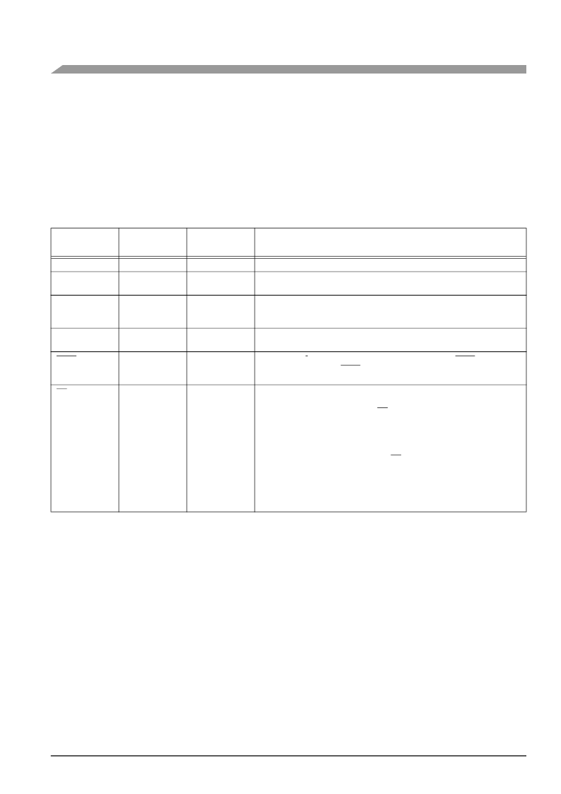
Table 1-15.
JTAG/OnCE Interface
Signal
Name
Type
State During
Reset
Signal Description
TCK
Input
Input
Test Clock
—A test clock input signal to synchronize the JTAG test logic.
TDI
Input
Input
Test Data Input
—A test data serial input signal for test instructions and data.
TDI is sampled on the rising edge of TCK and has an internal pull-up resistor.
TDO
Output
Tri-stated
Test Data Output
—A test data serial output signal for test instructions and
data. TDO is actively driven in the shift-IR and shift-DR controller states. TDO
changes on the falling edge of TCK.
TMS
Input
Input
Test Mode Select
—Sequences the test controller’s state machine. TMS is
sampled on the rising edge of TCK and has an internal pull-up resistor.
TRST
Input
Input
Test Reset
—Initializes the test controller asynchronously. TRST has an
internal pull-up resistor. TRST must be asserted during and after power-up
(see EB610/D for details).
DE
Input/ Output
Input
Debug Event
—As an input, initiates Debug mode from an external command
controller, and, as an open-drain output, acknowledges that the chip has
entered Debug mode. As an input, DE causes the DSP56300 core to finish
executing the current instruction, save the instruction pipeline information,
enter Debug mode, and wait for commands to be entered from the debug
serial input line. This signal is asserted as an output for three clock cycles
when the chip enters Debug mode as a result of a debug request or as a result
of meeting a breakpoint condition. The DE has an internal pull-up resistor.
This signal is not a standard part of the JTAG TAP controller. The signal
connects directly to the OnCE module to initiate debug mode directly or to
provide a direct external indication that the chip has entered Debug mode. All
other interface with the OnCE module must occur through the JTAG port.
相關(guān)PDF資料 |
PDF描述 |
|---|---|
| DSP56321VF200 | 24-Bit Digital Signal Processor |
| DSP56321VF220 | 24-Bit Digital Signal Processor |
| DSP56321VF240 | 24-Bit Digital Signal Processor |
| DSP56321VF275 | 24-Bit Digital Signal Processor |
| DSP56321VL200 | 24-Bit Digital Signal Processor |
相關(guān)代理商/技術(shù)參數(shù) |
參數(shù)描述 |
|---|---|
| DSP56321EVM | 功能描述:開發(fā)板和工具包 - 其他處理器 DSP56321EVM RoHS:否 制造商:Freescale Semiconductor 產(chǎn)品:Development Systems 工具用于評(píng)估:P3041 核心:e500mc 接口類型:I2C, SPI, USB 工作電源電壓: |
| DSP56321EVMUM | 制造商:未知廠家 制造商全稱:未知廠家 功能描述:DSP56321 EVM User's Manual |
| DSP56321FC200 | 制造商:Freescale Semiconductor 功能描述:HIP7 56321 200MHZ DSP - Trays |
| DSP56321FC220 | 制造商:Rochester Electronics LLC 功能描述:- Bulk |
| DSP56321RMAD | 制造商:未知廠家 制造商全稱:未知廠家 功能描述:DSP56321 Reference Manual Addendum |
發(fā)布緊急采購(gòu),3分鐘左右您將得到回復(fù)。