- 您現(xiàn)在的位置:買(mǎi)賣IC網(wǎng) > PDF目錄361638 > V30MZ V30MZ(TM) Hardware (Preliminary) | User's Manual[01/2002] PDF資料下載
參數(shù)資料
| 型號(hào): | V30MZ |
| 英文描述: | V30MZ(TM) Hardware (Preliminary) | User's Manual[01/2002] |
| 中文描述: | V30MZ(TM)硬件(初步)|用戶手冊(cè)[01/2002] |
| 文件頁(yè)數(shù): | 48/89頁(yè) |
| 文件大?。?/td> | 418K |
| 代理商: | V30MZ |
第1頁(yè)第2頁(yè)第3頁(yè)第4頁(yè)第5頁(yè)第6頁(yè)第7頁(yè)第8頁(yè)第9頁(yè)第10頁(yè)第11頁(yè)第12頁(yè)第13頁(yè)第14頁(yè)第15頁(yè)第16頁(yè)第17頁(yè)第18頁(yè)第19頁(yè)第20頁(yè)第21頁(yè)第22頁(yè)第23頁(yè)第24頁(yè)第25頁(yè)第26頁(yè)第27頁(yè)第28頁(yè)第29頁(yè)第30頁(yè)第31頁(yè)第32頁(yè)第33頁(yè)第34頁(yè)第35頁(yè)第36頁(yè)第37頁(yè)第38頁(yè)第39頁(yè)第40頁(yè)第41頁(yè)第42頁(yè)第43頁(yè)第44頁(yè)第45頁(yè)第46頁(yè)第47頁(yè)當(dāng)前第48頁(yè)第49頁(yè)第50頁(yè)第51頁(yè)第52頁(yè)第53頁(yè)第54頁(yè)第55頁(yè)第56頁(yè)第57頁(yè)第58頁(yè)第59頁(yè)第60頁(yè)第61頁(yè)第62頁(yè)第63頁(yè)第64頁(yè)第65頁(yè)第66頁(yè)第67頁(yè)第68頁(yè)第69頁(yè)第70頁(yè)第71頁(yè)第72頁(yè)第73頁(yè)第74頁(yè)第75頁(yè)第76頁(yè)第77頁(yè)第78頁(yè)第79頁(yè)第80頁(yè)第81頁(yè)第82頁(yè)第83頁(yè)第84頁(yè)第85頁(yè)第86頁(yè)第87頁(yè)第88頁(yè)第89頁(yè)
CHAPTER 4 BUS CONTROL FUNCTIONS
48
(2) When accessing word data at even address
Word data is accessed in 1-bus cycle with UBEB = 0 and A0 = 0.
Table 4-1 shows the relationship between the type of operand and the number of UBEB, A0 pins, and bus cycles.
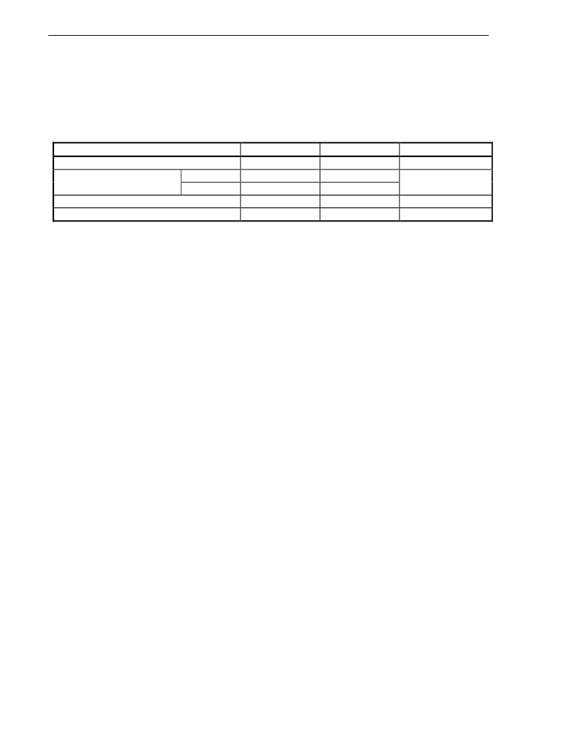
Table 4-1. V30MZ Data Access
Operand
UBEB pin output level
A0 pin output level
Number of Bus Cycles
Word at even address
L
L
1
Word at odd address
1st bus cycle
L
H
2
2nd bus cycle
H
L
Byte at even address
H
L
1
Byte at odd address
L
H
1
Remark
L : low level
H : high level
Normally, the V30MZ performs an access (prefetch) of an operation code in word units. However, when a branch
to an odd address takes place, only 1 byte at that odd address is fetched and subsequent bytes are fetched again in
word units again.
When a vector table address is generated from the vector number (0 to 225), an even address is always
generated, and so an access to the interrupt vector table is always performed as word data at an even address.
Therefore, a vector table access to one interrupt is always performed in 2 bus cycles for the 2 words of the segment
base and offset.
4.1.1 Cautions on accessing word data
When accessing word data by the V30MZ, ensure that all the data that can be checked by the program may be
placed at an even address. When it is placed at an odd address, the result will be as follows.
One bus cycle for a memory access requires 1 clock. Therefore, every time word data at an odd address is
accessed, one extra clock of the instruction execution time are required compared to accessing word data at an even
address. This applies when executing an instruction that has more than one word data access.
In the case of a word data transfer from memory to memory, 2 memory accesses are required for a read from the
source and a write to the destination and so the execution time becomes the maximum when both are odd
addresses.
This problem of odd addresses also happens in stack manipulation. Registers, etc. are automatically saved to the
stack by interrupt servicing, but these are all word data and so when processed at an odd address, note that the
number of bus cycles is doubled and the interrupt response time is delayed.
Example:
Number of execution clocks of MOV reg, mem instruction
Byte data : 1
Word data : 2 (For odd address)
: 1 (For even address)
This is an example in which one word data access is performed.
相關(guān)PDF資料 |
PDF描述 |
|---|---|
| V32FB-V42D-MMMME | MODEM Chip Set |
| DSP16A-F14-033 | 16-Bit Digital Signal Processor |
| DSP16A-F14-033I | 16-Bit Digital Signal Processor |
| DSP16A-F14-055 | 16-Bit Digital Signal Processor |
| DSP16A-F14-055I | 16-Bit Digital Signal Processor |
相關(guān)代理商/技術(shù)參數(shù) |
參數(shù)描述 |
|---|---|
| V30N | 制造商:Renesas Electronics Corporation 功能描述: |
| V-30TB | 制造商:Mencom 功能描述: |
| V31 | 制造商:SMC Corporation of America 功能描述:CONNECTOR |
| V3-1 | 功能描述:基本/快動(dòng)開(kāi)關(guān) 15.1A pin plunger Screw Terminals RoHS:否 制造商:Omron Electronics 觸點(diǎn)形式:SPDT 執(zhí)行器:Lever 電流額定值:5 A 電壓額定值 AC:250 V 電壓額定值 DC:30 V 功率額定值: 工作力:120 g IP 等級(jí):IP 67 NEMA 額定值: 端接類型:Wire 安裝:Panel |
| V3-1001 | 功能描述:基本/快動(dòng)開(kāi)關(guān) Snap Action SPDT 10A 3.89N Thru-Hole RoHS:否 制造商:Omron Electronics 觸點(diǎn)形式:SPDT 執(zhí)行器:Lever 電流額定值:5 A 電壓額定值 AC:250 V 電壓額定值 DC:30 V 功率額定值: 工作力:120 g IP 等級(jí):IP 67 NEMA 額定值: 端接類型:Wire 安裝:Panel |
發(fā)布緊急采購(gòu),3分鐘左右您將得到回復(fù)。