- 您現(xiàn)在的位置:買賣IC網 > PDF目錄199479 > TSB43AA82PGE (TEXAS INSTRUMENTS INC) 2 CHANNEL(S), 400M bps, SERIAL COMM CONTROLLER, PQFP144 PDF資料下載
參數(shù)資料
| 型號: | TSB43AA82PGE |
| 廠商: | TEXAS INSTRUMENTS INC |
| 元件分類: | 微控制器/微處理器 |
| 英文描述: | 2 CHANNEL(S), 400M bps, SERIAL COMM CONTROLLER, PQFP144 |
| 封裝: | PLASTIC, QFP-144 |
| 文件頁數(shù): | 49/146頁 |
| 文件大?。?/td> | 770K |
| 代理商: | TSB43AA82PGE |
第1頁第2頁第3頁第4頁第5頁第6頁第7頁第8頁第9頁第10頁第11頁第12頁第13頁第14頁第15頁第16頁第17頁第18頁第19頁第20頁第21頁第22頁第23頁第24頁第25頁第26頁第27頁第28頁第29頁第30頁第31頁第32頁第33頁第34頁第35頁第36頁第37頁第38頁第39頁第40頁第41頁第42頁第43頁第44頁第45頁第46頁第47頁第48頁當前第49頁第50頁第51頁第52頁第53頁第54頁第55頁第56頁第57頁第58頁第59頁第60頁第61頁第62頁第63頁第64頁第65頁第66頁第67頁第68頁第69頁第70頁第71頁第72頁第73頁第74頁第75頁第76頁第77頁第78頁第79頁第80頁第81頁第82頁第83頁第84頁第85頁第86頁第87頁第88頁第89頁第90頁第91頁第92頁第93頁第94頁第95頁第96頁第97頁第98頁第99頁第100頁第101頁第102頁第103頁第104頁第105頁第106頁第107頁第108頁第109頁第110頁第111頁第112頁第113頁第114頁第115頁第116頁第117頁第118頁第119頁第120頁第121頁第122頁第123頁第124頁第125頁第126頁第127頁第128頁第129頁第130頁第131頁第132頁第133頁第134頁第135頁第136頁第137頁第138頁第139頁第140頁第141頁第142頁第143頁第144頁第145頁第146頁
142
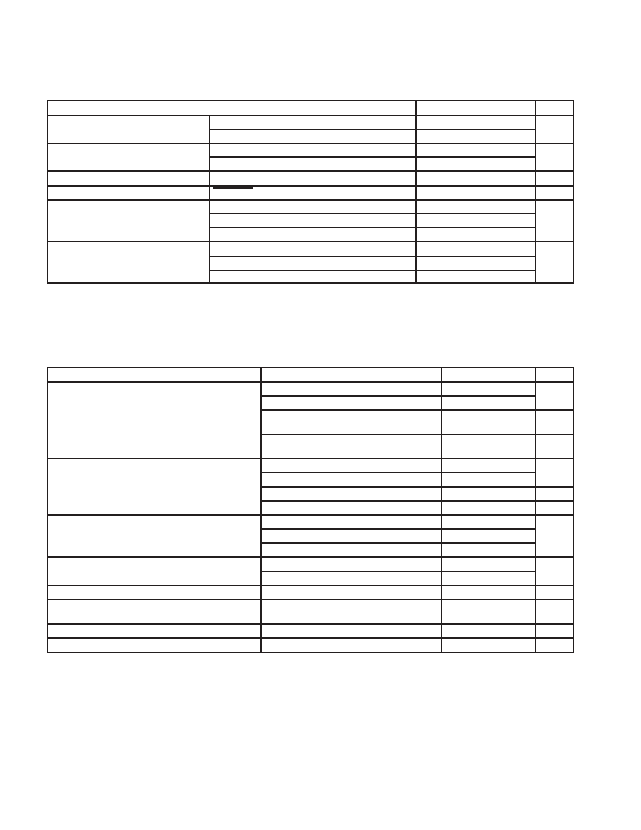
14.2 Recommended Operating Conditions (continued)
MIN
NOM
MAX
UNIT
Differential input voltage, VID
Cable inputs, during data reception
118
260
mV
Differential input voltage, VID
Cable inputs, during arbitration
168
265
mV
Common-mode input voltage, VIC
TPB cable inputs, source power node
0.4706
2.515
V
Common-mode input voltage, VIC
TPB cable inputs, nonsource power node
0.4706
2.015
V
Output current, IO
TPBIAS outputs
–5.6
1.3
mA
Power-up reset time, tpu
XRESETP input
2
ms
TPA, TPB cable inputs, S100 operation
±1.08
Receive input jitter
TPA, TPB cable inputs, S200 operation
±0.5
ns
Receive input jitter
TPA, TPB cable inputs, S400 operation
±0.315
ns
Between TPA and TPB cable inputs, S100 operation
±0.8
Receive input skew
Between TPA and TPB cable inputs, S200 operation
±0.55
ns
Receive input skew
Between TPA and TPB cable inputs, S400 operation
±0.5
ns
For a node that does not source power, see Section 4.2.2.2 in IEEE P1394a.
14.3 Electrical Characteristics Over Recommended Ranges of Operating Conditions
(Unless Otherwise Noted)
14.3.1 Device
PARAMETER
TEST CONDITIONS
MIN
TYP
MAX
UNIT
PLLON/PD/LPS/ENZ = L/L/L/L, PWTST = NC
2.1
mA
PLLON/PD/LPS/ENZ = H/L/L/L, PWTST = NC
11.2
mA
IDD-ULP
Supply current—ULP (ultralow power)
(see Note 1)
PLLON/PD/LPS/ENZ = L/L/L/H,
51
A
IDD-ULP
Supply current—ULP (ultralow power)
(see Note 1)
PLLON/PD/LPS/ENZ = L/L/L/H,
PWTST = 1.8 V
51
A
(see Note 1)
PLLON/PD/LPS/ENZ = H/L/L/H,
9.3
mA
PLLON/PD/LPS/ENZ = H/L/L/H,
PWTST = 1.8 V
9.3
mA
PLLON/PD/LPS/ENZ = L/H/X/L
2.1
mA
IDD-PD
Supply current—PD (power down)
PLLON/PD/LPS/ENZ = H/H/X/L
11.0
mA
IDD-PD
Supply current—PD (power down)
(see Note 2)
PLLON/PD/LPS/ENZ = L/H/X/H
51
Α
(see Note 2)
PLLON/PD/LPS/ENZ = H/H/X/H
9.3
mA
Supply current—(PLLON/PD/LPS/ENZ =
Ports disabled
30.4
Supply current—(PLLON/PD/LPS/ENZ =
X/L/H/L)
One port enabled
46.6
mA
IDD
X/L/H/L)
Two ports enabled
62.6
mA
IDD-op
Supply current—transmitting/receiving
One port enabled
48.0
mA
IDD-op
Supply current—transmitting/receiving
16 bit data through BDI (packets 512 bytes)
Two ports enabled
64.0
mA
VTH
Power status threshold, CPS input
400-k
resistor
4.7
7.5
V
II
Input current, LPS, PD, PHYTESTM,
PWRCLS
[0:2]
VDD = 3.6-V
5
A
IIRST
Pullup current, XRESETP input
VI = 1.5-V or 0-V
–90
–20
A
VO
TPBIAS output voltage
At rated IO current
1.665
2.015
V
NOTES:
1. Ultralow-power (LPS = L): Using LPS to enable a low-power mode allows the user not to provide a reset when disabling the
low-power mode. In this mode, the user must provide the 1.8-V core voltage, externally (ENZ = H, PWTST = 1.8 V) or internally
(ENZ = L, PWTST = NC, decoupling caps).
2. Power-down mode (PD = H): When power-down mode is disabled, a reset must be applied to the device.
相關PDF資料 |
PDF描述 |
|---|---|
| TSB43AA82GGW | 2 CHANNEL(S), 400M bps, SERIAL COMM CONTROLLER, PBGA176 |
| TSB43DA42GHCR | PCI BUS CONTROLLER, PBGA196 |
| TSB500SK02 | 30 A, BARRIER STRIP TERMINAL BLOCK, 1 ROW, 1 DECK |
| TSB500SK10MDS | 30 A, BARRIER STRIP TERMINAL BLOCK, 1 ROW, 1 DECK |
| TSB5000331DS | 30 A, BARRIER STRIP TERMINAL BLOCK, 1 ROW, 1 DECK |
相關代理商/技術參數(shù) |
參數(shù)描述 |
|---|---|
| TSB43AA82PGEG4 | 功能描述:1394 接口集成電路 2Port Hi Per Int Phy & Link Layer Chip RoHS:否 制造商:Texas Instruments 類型:Link Layer Controller 工作電源電壓: 封裝 / 箱體:LQFP 封裝:Tray |
| TSB43AB21 | 制造商:TI 制造商全稱:Texas Instruments 功能描述:INTERGRATED 1394A-2000 OHCI PHY LINK-LAYER CONTROLLER |
| TSB43AB21A | 制造商:TI 制造商全稱:Texas Instruments 功能描述:Integrated 1394a-2000 OHCI PHY/Link-Layer Controller |
| TSB43AB21A-EP | 制造商:未知廠家 制造商全稱:未知廠家 功能描述:Military Enhanced Plastic Integrated 1394a-2000 OCHI pHY/Link-Layer Controller |
| TSB43AB21AI | 制造商:TI 制造商全稱:Texas Instruments 功能描述:Integrated 1394a-2000 OHCI PHY/Link-Layer Controller |
發(fā)布緊急采購,3分鐘左右您將得到回復。