- 您現(xiàn)在的位置:買賣IC網(wǎng) > PDF目錄192292 > S19237PB13 (APPLIEDMICRO INC) TRANSCEIVER, PBGA255 PDF資料下載
參數(shù)資料
| 型號(hào): | S19237PB13 |
| 廠商: | APPLIEDMICRO INC |
| 元件分類: | 數(shù)字傳輸電路 |
| 英文描述: | TRANSCEIVER, PBGA255 |
| 封裝: | PLASTIC, BGA-255 |
| 文件頁數(shù): | 46/60頁 |
| 文件大小: | 1418K |
| 代理商: | S19237PB13 |
第1頁第2頁第3頁第4頁第5頁第6頁第7頁第8頁第9頁第10頁第11頁第12頁第13頁第14頁第15頁第16頁第17頁第18頁第19頁第20頁第21頁第22頁第23頁第24頁第25頁第26頁第27頁第28頁第29頁第30頁第31頁第32頁第33頁第34頁第35頁第36頁第37頁第38頁第39頁第40頁第41頁第42頁第43頁第44頁第45頁當(dāng)前第46頁第47頁第48頁第49頁第50頁第51頁第52頁第53頁第54頁第55頁第56頁第57頁第58頁第59頁第60頁
50
DS1454
AMCC Confidential and Proprietary
S19237 – SONET STS-192/10GbE CMOS Transceiver
with ISI Compensation
Data Sheet
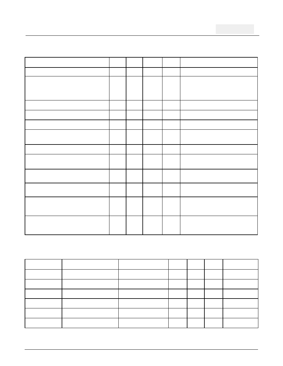
Table 24. Recommended Operating Conditions
The device will meet all electrical specifications at junction temperature under bias of 125C but part lifetime and reliability will be reduced. It is recommended that
prudent thermal management techniques are used to maximize device lifetime.
Parameter
Min
Typ
Max
Units
Conditions
Ambient temperature under bias
-40
+85
°C
Junction temperature under bias
105
125
°C
Note: AMCC recommends that the
device is predominantly operated at or
below the specified typical junction
temperature.
Voltage on VDD_1.2aV with respect to GND
1.14
1.20
1.26
V
All +1.2V Supplies Minus AVDD_RX
Voltage on VDD_1.2bV with respect to GND
1.10a
1.20
1.26
V
AVDD_RX Power Supply Only
Voltage on VDD_1.8 V with respect to GND
1.71
1.80
1.89
V
Voltage on VDD_1.8 V with respect to GND
(when using a 3.3 V supply)
3.135
3.3
3.465
V
ICC_1.2 V supply current
733
899
mA
ICC_1.8 V supply current (with 1.8 V or 3.3
V supply)
87
114
mA
Power dissipation (when using 1.2 V and
1.8 V supplies)
1.037
1.349b
W
Power dissipation (when using 1.2 V and
3.3 V supplies)
1.167
1.529b
W
Power supply noise rejection for 1.2 V
power supply
(6 kHz – 2 MHz)
50
mVP-P
Power supply noise rejection for 1.8 V
power supply
(6 kHz – 2 MHz)
50
mVP-P
a.Consult application note AN2087, Extended Low-End VCO Margin, for additional details. See Table 19 for VDD_1.2bV pin assignments/descriptions.
b.Use maximum Power Dissipation and Table 21 for Thermal Management considerations.
Table 25. LVCMOS Input/Output Characteristics
Parameter
Description
Min
Typ
Max
Units
Conditions
VIH
Input high-voltage
VDD_1.8 CMOS - 0.4
V
VIL
Input low-voltage
0.4
V
IIH
Input high current
60
A
IIL
Input low current
60
A
VOH
Output high-voltage
VDD_1.8 CMOS - 0.2
V
IOH = -600 A
VOL
Output low-voltage
0.2
V
IOL = 600 A
相關(guān)PDF資料 |
PDF描述 |
|---|---|
| S1950E-FREQ-OUT25 | CRYSTAL OSCILLATOR, CLOCK, 80 MHz - 125 MHz, ACMOS OUTPUT |
| S1F78100Y2A0 | 6 V FIXED POSITIVE REGULATOR, PSSO3 |
| S1F78100Y2B0 | 5 V FIXED POSITIVE REGULATOR, PSSO3 |
| S1F78100Y2C0 | 3.2 V FIXED POSITIVE REGULATOR, PSSO3 |
| S1F78100Y2F0 | 2.2 V FIXED POSITIVE REGULATOR, PSSO3 |
相關(guān)代理商/技術(shù)參數(shù) |
參數(shù)描述 |
|---|---|
| S19237PB13-2 | 制造商:AppliedMicro 功能描述: |
| S19237PBICC | 制造商:AppliedMicro 功能描述:IC INTERFACE TRANSCEIVER LOW POWER CMOS 255 BGA 制造商:AMCC 功能描述: |
| S19238CBI | 制造商:AppliedMicro 功能描述: |
| S19250 | 制造商:AMCC 制造商全稱:Applied Micro Circuits Corporation 功能描述:STS-192 SONET/SDH/FEC/GbE/FC 16-bit Transceiver with EDC |
| S19250PBIC | 制造商:AppliedMicro 功能描述:10G SERDES EDC/SFI-4 |
發(fā)布緊急采購(gòu),3分鐘左右您將得到回復(fù)。